PAD188 – Rev F
KEY FEATURES
- LOW COST
- SMALL SIZE 31.5mm SQUARE
- HIGH VOLTAGE – 525 VOLTS
- OUTPUT CURRENT– 100mA
- 5 WATT DISSIPATION CAPABILITY
- 3V/µS SLEW RATE
- 1mA QUIESCENT CURRENT
- RoHS COMPLIANT
APPLICATIONS
- HIGH VOLTAGE INSTRUMENTATION
- PIEZO TRANSDUCER DRIVE
- ELECTRON BEAM FOCUSING
- PROGRAMMABLE VOLTAGE SOURCE
DESCRIPTION
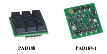
The PAD188 compact high voltage op amp is constructed with surface mount components to provide a cost-effective solution for many industrial applications such as high voltage instrumentation. With a footprint only 31.5mm square the PAD188 offers outstanding performance that rivals or exceeds more expensive hybrid components. Integrated passive heat sink cooling is included. User selectable external compensation tailors the amplifier’s response to the application requirements. A single resistor programs the current limit feature. The PAD188 is built on a thermally conductive but electrically insulating substrate. No BeO is used in the PAD188. For very low power applications the PAD188-1 version of the amplifier is available without the integrated heat sink. The circuit is conformal coated for additional safety and reliability. See “CONFORMAL COATING” paragraph on page 5.
A NEW CONCEPT
A critical task in any power amplifier application is cooling the amplifier. Until now component amplifier manufacturers often treated this task as an after-thought, left for the user to figure out. At Power Amp Design the best heat sink is chosen at the start and becomes an integral part of the overall amplifier design. The result is the most compact and volumetric efficient design combination at the lowest cost. In addition, this integrated solution concept offers an achievable real-world power dissipation rating, not the ideal rating usually cited when the amplifier case is somehow kept at 25℃. The user no longer needs to specify, procure or assemble separate components.
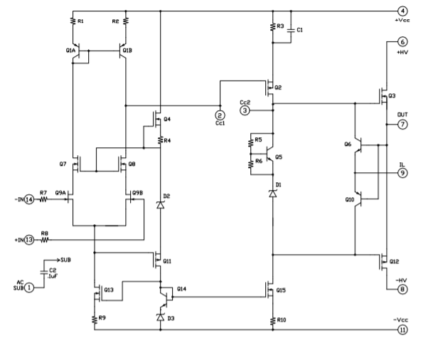
CIRCUIT & CONNECTIONS
EQUIVALENT CIRCUIT
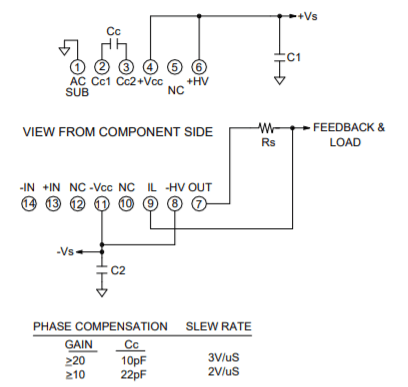
PINOUT & CONNECTIONS
ABSOLUTE MAXIMUM RATINGS SPECIFICATIONS
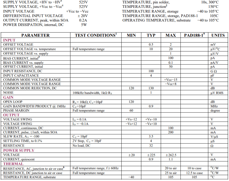
NOTES:
- Unless otherwise noted: TC = 25℃, compensation Cc = 150pF, DC input specifications are ± value given, power supply voltage is typical rating.
- Derate internal power dissipation to achieve high MTBF.
- Doubles for every 10℃ of case temperature increase.
- +HV and −HV denote the positive and negative supply voltages to the output stage. +Vcc and –Vcc denote the positive and negative supply voltages to
the small signal stages. +Vcc and –Vcc may not be more than + and – 20V greater than +HV and –HV respectively. - Rating applies if the output current alternates between both output transistors at a rate faster than 60Hz.
- Power supply voltages +Vcc and −Vcc must not be less than +HV and −HV respectively. Total voltage +Vcc to −Vcc 525V maximum.
- Specifications for the PAD188-1 are the same as for the PAD188 except as shown in this column.
OPERATING CONSIDERATIONS
SAFETY FIRST
The operating voltages of the PAD188 are potentially deadly. When developing an application circuit it is wise to begin with power supply voltages as low as possible while checking for circuit functionality. Increase supply voltages slowly as confidence in the application circuit increases. Always use a “hands-off” method whereby test equipment probes are attached or handled only when power is off.
MOUNTING THE AMPLIFIER
In many applications for the PAD188 little to no output current is required. In this case the PAD188-1 (no heat sink version) can be used since the maximum quiescent power dissipation is only about 525mW. In other applications the output current may be such that several watts of internal power dissipation capability is required. In this case the PAD188 is better suited for the application because of the integrated heat sink. In either case follow the notes on the pages for “Dimensional Information”
PHASE COMPENSATION
The PAD188 must be phase compensated. The compensation capacitor, CC, is connected between pins 2 and 3. The
compensation capacitor must be an NPO type capacitor rated for the full supply voltage (500V). On page 2, under Amplifier Pinout and Connections, you will find a table that gives recommended compensation capacitance value for various circuit gains and the resulting slew rate for each capacitor value. Consult also the small signal response and phase response plots for the selected compensation value in the Typical Performance Graphs section. A compensation
capacitor less than 10pF is not recommended.
EXTERNAL CIRCUIT COMPONENTS
The output of the PAD188 can swing over 500V and this may stress or destroy external components that are often not seriously considered when developing circuits with small signal op amps. For example, it is often overlooked that the usual voltage rating for metal film resistors is only 200V and that application circuits using the PAD188 may place over 500V across the feedback resistor. High voltage rated resistors may be purchased for the feedback circuit or, alternately, several ordinary resistors may be placed in series to obtain the proper voltage rating. We recommend at least three resistors in series for the feedback resistor. The compensation capacitor CC is a NPO type and is rated for 600V. The voltage rating of the connecting wire and PCB spacing between pads and connecting traces needs to be considered as well. See application note AN16 for details.
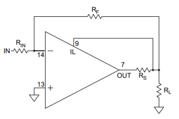
CURRENT LIMIT
Current limit can be programmed by attaching a suitable value resistor as shown in Figure 1. The value of the limited
current can be approximately calculated by:
IL=.65/RS
Where IL is the value of the limited current and RS is the value of the current sense resistor. It is important that the type of resistor chosen for RS be non-inductive. A wire-wound resistor is not a good choice even if it is rated as “non inductive” since it will exhibit significant inductance at some frequency. A better choice is a type of resistor that is more inherently non-inductive such as a metal film resistor or a thick film resistor. The current limit circuitry works by diverting the stage currents of the amplifier into the output circuit (about 0.4mA) and this introduces an error term compared to the approximate equation given above. As the current limit value is reduced the proportion of the error term increases. The practical range of current limit is from 100mA to 2mA. The current limit decreases 2.2mV/℃ with increasing temperature since the sense voltage for calculating the current limit is the emitter-base circuit of a bipolar transistor.
Current Limit
INPUT PROTECTION
In applications where the input differential voltage may be exceeded (dc or transient) it is important to add differential input voltage protection. See Figure 2.
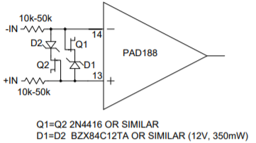
Input differential voltage protection
It is important that the power supply connections to the PAD188 not be open. If for example, the negative supply connection were to open, the internal circuitry of the amplifier will bootstrap the amplifier to the positive supply through the feedback gain-setting resistor. When the +IN is grounded the input circuit is clamped to ground while the output of the amplifier will float to the positive supply voltage via the bootstrapping effect. The input differential voltage of the amplifier may be exceeded, destroying the input stage. This is one good reason to protect the input as shown in Figure 2. But it is also a good reason to clamp the power supply pins as shown in Figure 3 below.
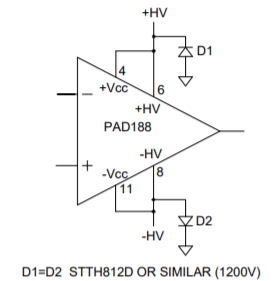
Power supply clamps
CONFORMAL COATING
The circuit of the PAD188 is covered by a silicone conformal coating for extra protection against internal arcing and environmental considerations such as humidity. The conformal coating is soft and may be damaged by rough handling. It is therefore recommended that the circuit be handled only by the edges of the substrate to avoid disturbing the coating. The PAD188 is only rated for normal environmental conditions of atmospheric pressure, humidity and temperature usually found in a laboratory or production floor. The user must make appropriate steps to insure the reliability of the application circuit beyond those conditions.
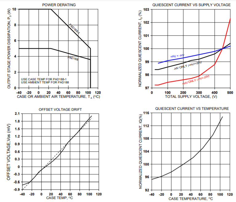
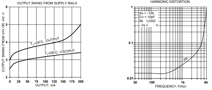
TYPICAL PERFORMANCE GRAPHS
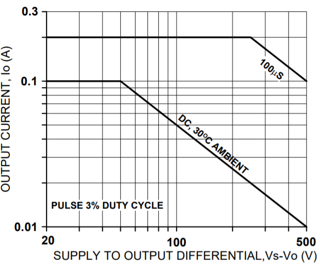
SAFE OPERATING AREA
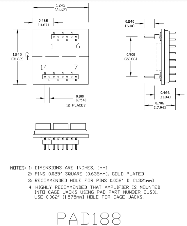
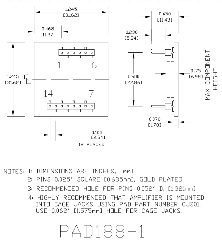
DIMENSIONAL INFORMATION
APPLICATION CIRCUITS
APPLICATION CIRCUIT
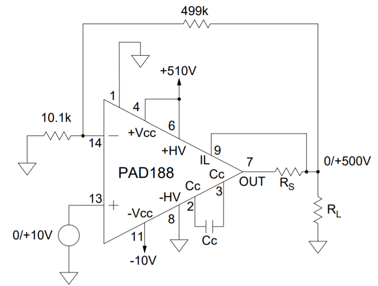
500V PROGRAMMABLE VOLTAGE SOURCE