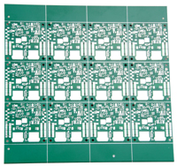
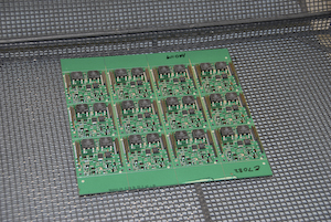
Our automated manufacturing assembly process begins with a multi-circuit panel. The circuit has been printed on an insulated metal substrate. The base material of the panel is usually aluminum but copper is also used for some models. The insulated metal substrate is characterized by thermal conductivity about 50 times higher than ordinary circuit board material and allows our products to dissipate high power levels not possible with standard circuit boards. The panel is scored so that individual circuits can be broken off at the completion of the automated assembly process. In this illustration of the manufacturing process we will follow the assembly of the PAD118 High Power Op Amp.
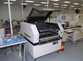
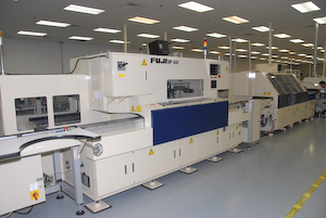
In the solder stenciling machine, solder paste is applied to the PAD118 panel by a squeegee forcing the solder paste through a metal stencil with cutouts the same size and shape as the component lead pads. This is similar to silk screen printing but with a metal stencil. Water soluable flux is mixed with small solder beads to form the solder paste.
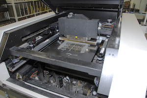
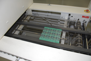
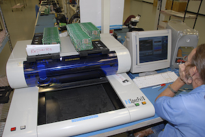
The next operation is “pick and place” where components are picked off reels and placed on the PAD118 panel by a high speed assembly machine. The pick and place machine can place well over 100 components per minute. The location of each component is programmed into the machine. The panel is attached to a table that moves X, Y, Z and angle under control of the program and a computerized vision system to correctly place each component.
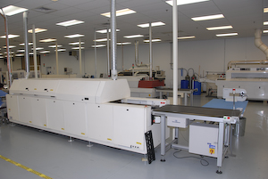
In the next process the PAD118 panel goes through a multi-zone furnace to reflow the solder. The soldering temperature is ramped up over time, spiked to the solder reflow temperature, held at the reflow temperature for approximately one minute, then cooled to near room temperature as the panel exits the furnace.
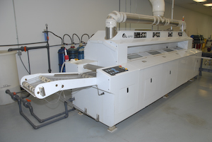
In this step of the manufacturing process the PAD118 panel is washed with de-ionized water to remove all solder flux residue.
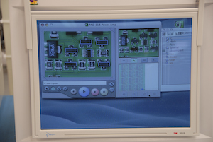
In the final step of the automated assembly process the PAD118 panel is inspected by a computerized vision system. A known good circuit is captured in the vision system and compared to a circuit under test. With a variety of lighting techniques such as laser illumination, the vision system can detect poor solder joints, missing components, wrong component values or incorrect component orientations as well as other defects.
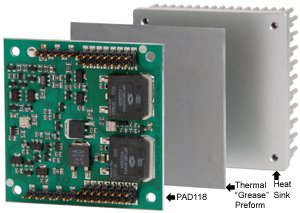
The next assembly steps are manual. The PAD118 substrate is bonded to the heat sink with a thermal “grease” preform. To begin with the preform is much thicker than necessary to fill in any gaps between the substrate and heat sink, but the exact thickness needed for each amplifier varies. The substrate is bonded to the heat sink by applying heat and pressure for 30 minutes. During this time the preform expands and flows. Excess material is squeezed out the edges of the assembly. The result is that all the air bubbles are squeezed out and all the gaps are filled in with “grease”. This is a superior bond as thick as it needs to be but no thicker than necessary. The final bond is typically 0.002″ [0.05mm] thick. After this step the fan is attached and the mounting studs added to complete the amplifier assembly.