PAD117A
Rev J
KEY FEATURES
- LOW COST RAIL TO RAIL INPUT & OUTPUT
- SINGLE SUPPLY OPERATION
- HIGH VOLTAGE – 100 VOLTS
- HIGH OUTPUT CURRENT – 15A
- 250 WATT OUTPUT CAPABILITY
- 100 WATT DISSIPATION CAPABILITY
- WIDE SUPPLY RANGE 5V – 50V
- INTEGRATED HEAT SINK AND FAN
- TEMPERATURE REPORTING
- OVER-TEMP SHUTDOWN
APPLICATIONS
- LINEAR MOTOR DRIVE
- INDUSTRIAL AUDIO
- SEMICONDUCTOR TESTING
- VIBRATION CANCELLATION
DESCRIPTION
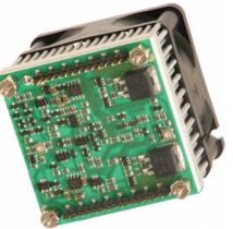
The PAD117A rail to rail operational amplifier is constructed with surface mount components to provide a cost effective solution for many industrial applications where it is important to obtain a maximum output signal with limited supply voltages. With a footprint only 5.6 in2 the PAD117A offers outstanding performance that rivals much more expensive hybrid component amplifiers or rack-mount amplifiers. User selectable external compensation tailors the amplifier’s response to the application requirements. Four-wire programmable current limit is built-in, but the PAD117A is compatible with the external PAD125 current limit accessory module as well. The PAD117A also features a substrate temperature reporting output and overtemp shutdown. The amplifier circuitry is built on a thermally conductive but electrically insulating substrate mounted to an integral heat sink and fan assembly. No BeO is used in the PAD117A. The resulting module is a small, high performance turn-key solution for many industrial applications.
A NEW CONCEPT
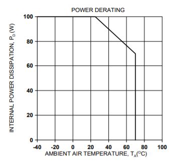
A critical task in any power amplifier application is cooling the amplifier. Until now component amplifier manufacturers often treated this task as an after-thought, left for the user to figure out. At Power Amp Design the best heat sink and fan combination is chosen at the start and becomes an integral part of the overall amplifier design. The result is the most compact and volumetric efficient design combination at the lowest cost. In addition, this integrated solution concept offers an achievable real-world power dissipation rating, not the ideal rating usually cited when the amplifier case is somehow kept at 25o C. The user no longer needs to specify, procure or assemble separate components.
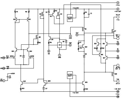
CIRCUIT & CONNECTIONS
EQUIVALENT CIRCUIT
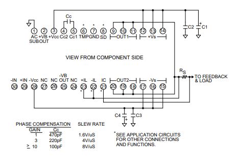
AMPLIFIER PINOUT & CONNECTIONS
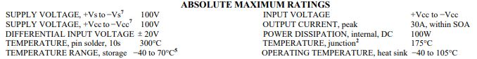
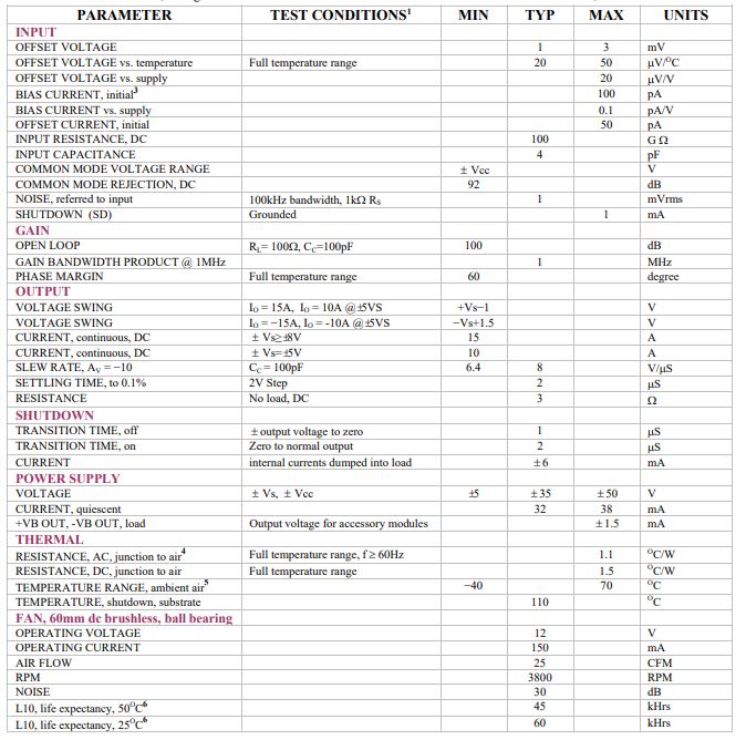
ABSOLUTE MAXIMUM RATINGS SPECIFICATIONS
NOTES:
- Unless otherwise noted: TC=25OC, compensation Cc=470pF, DC input specifications are value given, power supply voltage is typical rating.
- Derate internal power dissipation to achieve high MTBF.
- Doubles for every 10OC of case temperature increase.
- Rating applies if the output current alternates between both output transistors at a rate faster than 60Hz.
- Limited by fan characteristics. During operation, even though the heat sink may be at 85OC or more the fan will be at a lower temperature.
- L10 refers to the time it takes for 10% of a population of fans to fail. Lower ambient temperature increase fan life.
- +Vs and +Vcc tied together, -Vs and –Vcc tied together
OPERATING CONSIDERATIONS
COMMON MODE RANGE
The PAD117A is a rail to rail operational amplifier. This means that it works equally well with the input pins biased to either supply rail or at any voltage in between. The most common application utilizing this function is the single supply voltage amplifier where the +IN pin and the –Vs supply pin are grounded.
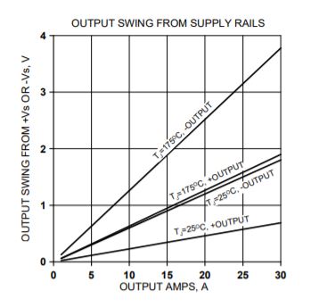
OUTPUT SWING
With no load the output voltage of the PAD117A can swing to either supply voltage rail. As the load current increases the maximum output swing is reduced, but at 15A output the swing from the positive supply rail is less than 1V and less than 1.5V from the negative supply rail. This does not include any voltage drop due to the sensing voltage required for the current limit circuit to operate.
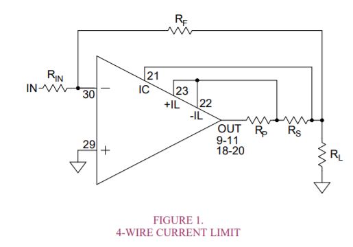
CURRENT LIMIT
The current limiting function of the PAD117A is a versatile circuit that can be used to implement a four-wire current limit configuration or, in combination with some external components can be configured to implement a fold-over current limit circuit. The four-wire current limit configuration insures that parasitic resistance in the output line, Rp, does not affect the programmed current limit setting. See Figure 1. The sense voltage for current limit is 0.65V. Thus:

Where IL is the value of the limited current and RS is the value of the current limit sense resistor.
In addition, the sense voltage has a temperature coefficient approximately equal to –2.2mV/o C. The fold-over function reduces the available current as the voltage across the output transistors increases to help insure that the SOA of the output transistors is not exceeded. Refer to Application Circuits for details on how to connect the current limit circuitry to implement either a four-wire current limit or current limit with a fold-over function.
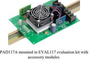
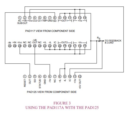
In some applications better current limiting protection and a lower sense voltage may be desired. In this case the PAD117A can be operated with the PAD125 current limit accessory module. See Figure 3 in the applications section and the PAD125 data sheet for more details.
COOLING FAN
The PAD117A relies on its fan for proper cooling of the amplifier. Make sure that air flow to the fan and away from the heat sink remains unobstructed. To eliminate electrical noise created by the cooling fan we recommend a 47µF capacitor placed directly at the point where the fan wires connect to the PCB. See application note AN-24 for further details.
MOUNTING THE AMPLIFIER
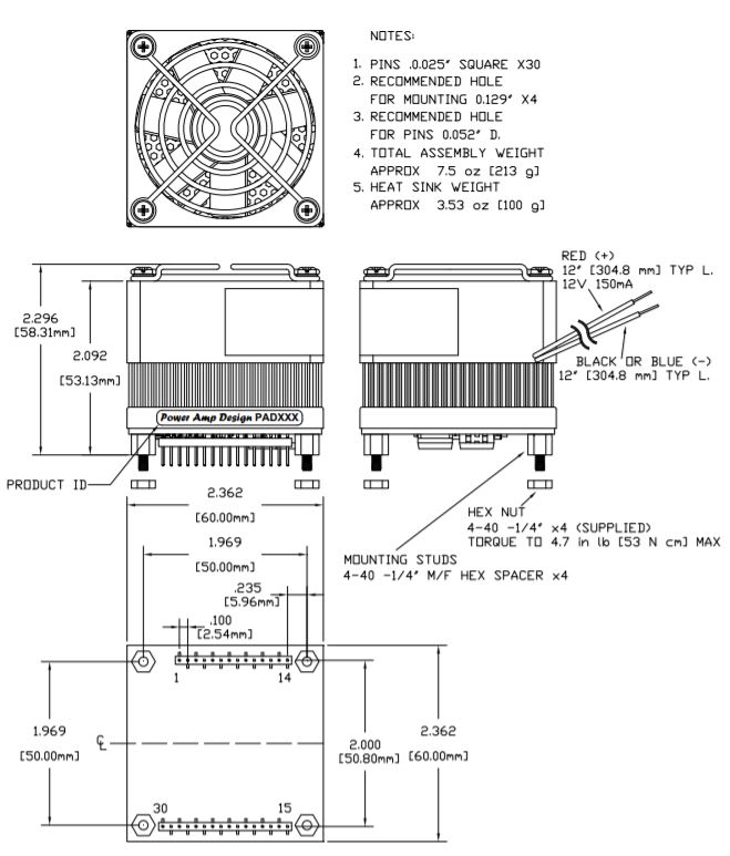
The amplifier is supplied with four 4-40 M/F hex spacers at the four corners of the amplifier. Since the male threaded ends
of the spacers extend beyond the amplifier pins the spacers provide a convenient alignment tool to guide the insertion of the amplifier pins into the circuit board. Once the amplifier is seated secure the module with the provided 4-40 nuts and torque to 4.7 in lb [53 N cm] max. See “Dimensional Information” for a detailed drawing. It is recommended that the heat sink be grounded to the system ground. This can easily be done by providing a grounded circuit board pad around any of the holes for the mounting studs.
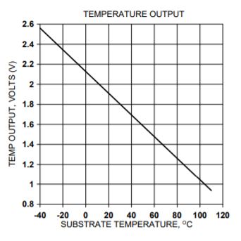
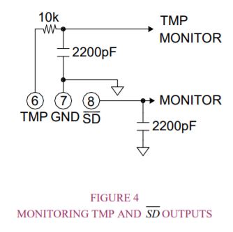
TEMPERATURE REPORTING
An analog output voltage is provided (pin 6, TMP) relative to ground and proportional to the temperature in degrees C. The slope is approximately -10.82mV/o C. The output voltage follows the equation:
T = (2.127 ─ V) (92.42)
Where V is the TMP output voltage and T is the substrate
temperature in degrees C.
This high impedance output circuit is susceptible to
capacitive loading and pickup from the output of the
amplifier. When monitoring TMP filter the voltage as
shown in Figure 4. See Applications Circuits.
THERMAL SHUTDOWN
The temperature monitoring circuit automatically turns off the output transistors when the substrate temperature reaches 110o C. When the substrate cools down 10o C the output is enabled once again. The thermal shutdown feature is activated either by amplifier overloads or a failure of the fan circuit.
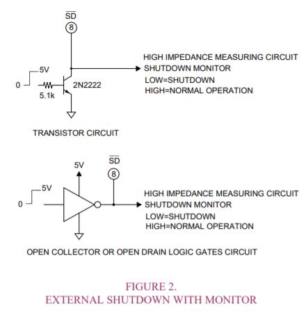
EXTERNAL SHUTDOWN
When pin 8 ( SD ) is taken low (ground) the output stage is turned “off” and remains “off” as long as pin 8 is low. When pin 8 is monitored with a high impedance circuit it also functions as a flag, reporting when the amplifier is shut down. A “high” (+5V) on pin 8 indicates the temperature is in the normal range. A “low” (ground) indicates a shutdown condition. See Application Circuits for details on how to implement an external shutdown circuit and how to monitor the shutdown status.
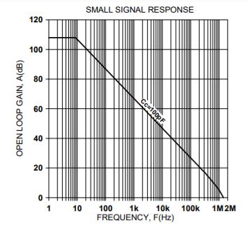
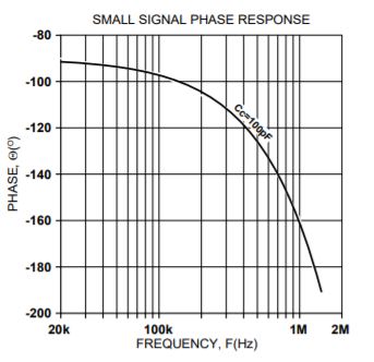
PHASE COMPENSATION
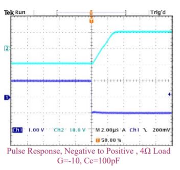
The PAD117A must be phase compensated to operate correctly. The compensation capacitor, CC, is connected between pins 4 and 5. On page 6, Typical Performance Graphs, you will find plots for small signal response and phase response using compensation values of 100pF and 470pF. The compensation capacitor must be an NPO type capacitor rated for the full supply voltage (100V). On page 2, under Amplifier Pinout and Connections, a table gives recommended compensation capacitance values for various gains and the resulting slew rate for each capacitor value.
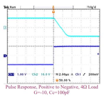
TYPICAL PERFORMANCE GRAPHS
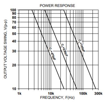
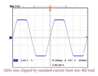
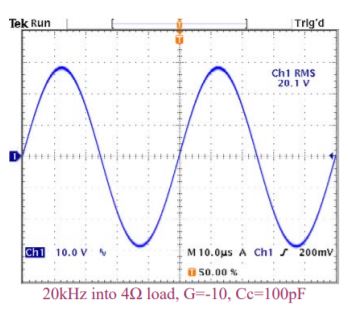
PERFORMANCE GRAPHS CONTINUED
SHUTDOWN RESPONSE, POSITIVE OUTPUT TO ZERO TRANSITION
The oscilloscope display at the right shows an expanded view of a 1kHz 1.2A p-p amplifier output signal being interrupted near the positive peak by a shutdown signal on Ch2. The Ch1 display shows the output current going to zero about 0.5µS after the shutdown signal goes low. The ringing in the output signal is due to inductance in the output line.
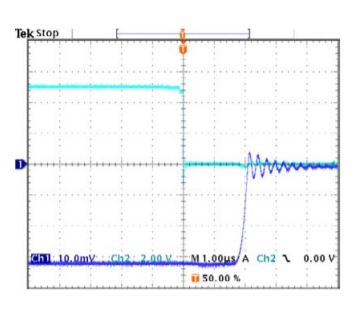
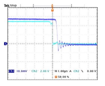
SHUTDOWN RESPONSE, NEGATIVE OUTPUT TO ZERO TRANSITION
The oscilloscope display at the left shows an expanded view of a 1kHz 1.2A p-p amplifier output signal being interrupted near the negative peak by a shutdown signal on Ch2. The Ch1 display shows the output current going to zero about 2µS after the shutdown signal goes low. The ringing in the output signal is due to inductance in the output line.
SAFE OPERATING AREA
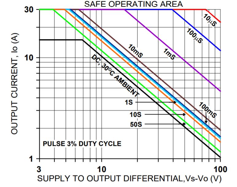
SAFE OPERATING AREA
The safe operating area (SOA) of a power amplifier is its single most important specification. The SOA graph presented above serves as a first approximation to help you decide if the PAD117A will meet the demands of your application. But a more accurate determination can be reached by making use of the PAD Power™ spreadsheet which can be found in the Power Amp Design website under the Design Spreadsheet tab. While the graph above adequately shows DC SOA and some pulse information it does not take into account ambient temperatures higher than 30OC, AC sine, phase or non-symmetric conditions that often appear in real-world applications. The PAD Power™ spreadsheet takes all of these effects into account.
DIMENSIONAL INFORMATION
APPLICATION CIRCUITS
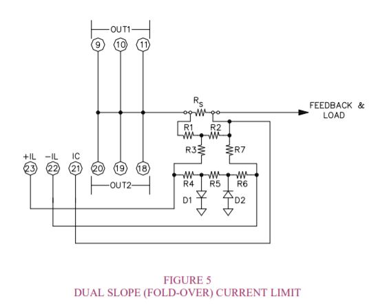
With the three current limit function pins (pins 21-23) dual slope current limiting can be implemented that more closely approximates the SOA curve of the amplifier than can be achieved with standard current limiting techniques. Values for resistors R1-R7 and RS can be calculated using the PAD Power™ spreadsheet that can be downloaded from the Power Amp Design web site under the Design Spreadsheet tab.