Downloads
Datasheet
EVAL188
Rev A
INTRODUCTION
The EVAL188 evaluation kit provides a convenient method to become familiar with the operation of amplifier model PAD188 before your application circuit is committed to production. Some assembly is required since user selections are needed depending on the application. For example, a current limit resistor value needs to be selected by the user. Also, there are two PCB mounting options available.
Critical connections for power supply bypassing and compensation are pre-wired. Terminal strips are also provided for input and output signals and power. A bread-boarding area is provided to construct the application circuit.
ASSEMBLY STEPS
Please note that the #1 cause of problems for evaluation kit users is not reading and following the directions (all of them). The #2 cause of problems is poor solder joints (cold or bridging). Don’t become a statistic. each step.
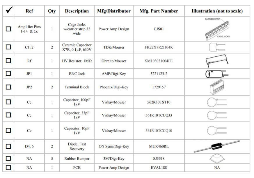
Refer to the Illustrated Parts List for the components mentioned in the assembly steps.
1. This evaluation kit is intended for use by professional engineers well familiar with the concerns of high voltage circuits. Be constantly aware that there are places on the circuit board where more than 500V may be exposed. On the circuit board these nodes are marked with a Δ symbol. Do not touch the circuit board unless you are sure the power supplies are turned off. Do not attach probes to the circuit unless the power is turned off. Be sure that any probes attached to the circuit can withstand over 500V. Do not leave the circuit unattended while powered up. While we have designed the board to be as safe as practical it is still your responsibility to guard your safety and that of others.
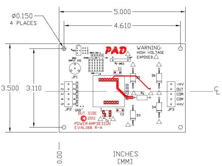
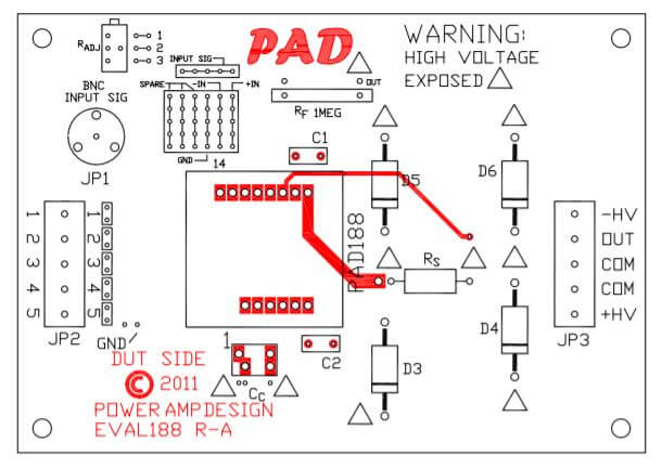
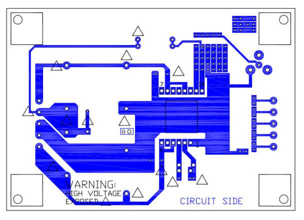
2. Notice that the printed circuit board (PCB) is labeled on one side as the “DUT SIDE” and the other side as “CIRCUIT” side.
3. Standard 1% metal film resistors may be used for the current limit sense resistor, Rs (not included in the kit but required for proper operation). See the datasheet for the amplifier to determine the best value for your application. Solder the resistor(s) from the “CIRCUIT SIDE” of the PCB.
4. The evaluation kit PCB can be mounted in two ways. Option 1- Chassis mount. Use #6 standoffs and screws (not supplied) attached to the PCB at the four corners of the PCB. Option 2- Bench-top mount. Use the five rubber bumpers supplied. These are “stick-on” components. Remove the release paper from each bumper and apply the bumper to the square outlines on the “CIRCUIT SIDE” of the PCB.
5. Be sure that the amplifier’s pin 1 aligns with pin 1 on the PCB. Slowly lower the amplifier into the PCB, making sure that the pins of the amplifier and the cage jacks mate. Push the amplifier into the PCB until it meets the PCB.
6. Notice that “Rf” is a 1 MΩ high voltage rated resistor. Over 500V may appear across this resistor and that much voltage may destroy normally rated components. If you need to replace this resistor with a component of some other value pay special attention to the voltage rating of that component.
7. Use the bread-boarding area to add the external components necessary to program the amplifier gain (noting that Rf is 1MΩ) and other circuit requirements to evaluate your application circuit. You can use the evaluation kit schematic and PCB views to map out your circuit.
8. Remember that the amplifier must be compensated to operate correctly. See the amplifier datasheet on Page 4, under PHASE COMPENSATION. The selected phase compensation capacitor will be installed at “CC” on the evaluation kit PCB. A 100pF capacitor has already been installed in your kit. Another value may better suit your application. Remove and replace the capacitor as necessary for your application. 10pF and 33pF capacitors are also included with the kit. CC must be rated for at least 500V. A temperature stable type capacitor is required—an X7R ceramic, for example, or an NPO type (preferred).
ASSEMBLY STEPS CONTINUED
9. The evaluation kit assembly is complete. Be sure you have read and followed all the assembly steps. Inspect the circuit board for solder shorts or poor solder joints. An illuminated magnifier is helpful. It is also helpful to use a solder with a water soluble flux and to wash and dry the board after your assembly is complete.
10. Note that the EVAL188 is intended for use in a lab type environment with normal atmospheric pressure, normal temperature and humidity conditions. Operation in other types of environments may lead to high voltage arching across circuit boards traces or circuit elements. The amplifier circuit itself is conformal coated except for the leads where the amplifier is connected to the user’s circuit board.
11. Before applying power to your circuit set the power supply for ±50V and set the power supply current limit to approximately 20mA. Use little or no load at first. Apply an input signal and check the output with an oscilloscope to verify proper functionality. This step can prevent damaging the amplifier or the circuit board should there be some mistake in assembly.
ILLUSTRATED PARTS LIST
Note that the amplifier is purchased separately.
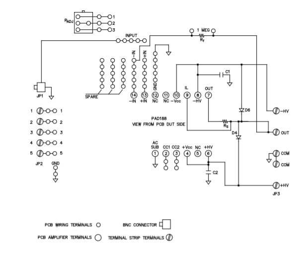
CIRCUIT & CONNECTIONS
CIRCUIT DIAGRAM
PCB VIEWS
TOP VIEW
BOTTOM VIEW
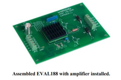
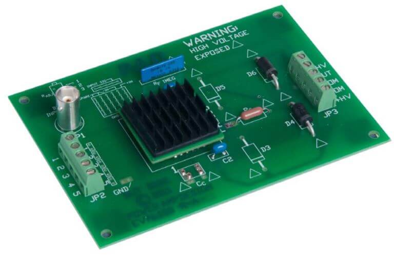
ASSEMBLED KIT
ASSEMBLED EVAL188 WITH AMPLIFIER INSTALLED
DIMENSIONAL INFORMATION
BOARD OUTLINE DIMENSIONS