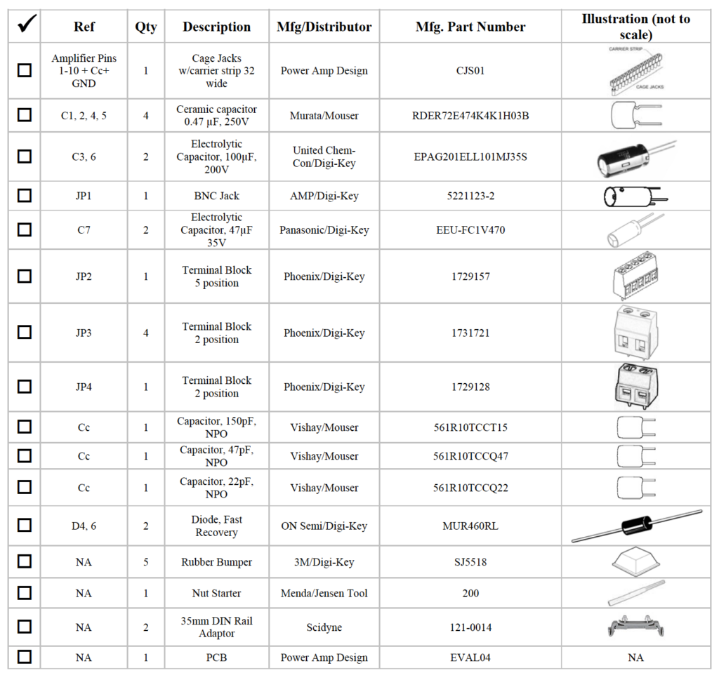
EVAL04
Rev A
INTRODUCTION
The EVAL04 evaluation kit provides a convenient method to become familiar with the operation of amplifier in the PAD04 series of amplifiers before your application circuit is committed to production. Some assembly is required since user selections are needed depending on the application. For example, there are several PCB mounting options available.
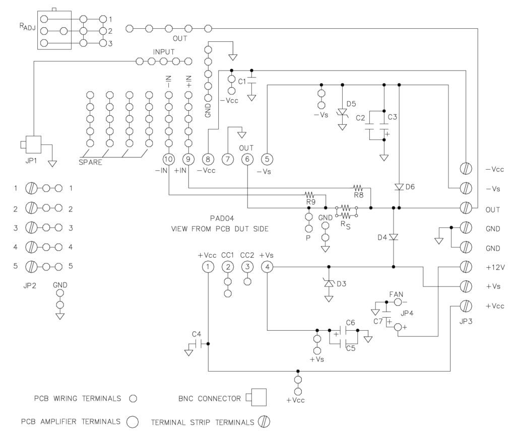
Critical connections for power supply bypassing and compensation are pre-wired. Connections are also provided for diode clamps on each power supply and the output for those applications in which significant inductive kickback may be found. Terminal strips are also provided for input and output signals and power.
ASSEMBLY STEPS
Please note that the #1 cause of problems for evaluation kit users is not reading and following the directions (all of them). The #2 cause of problems is poor solder joints (cold or bridging). Don’t become a statistic. each step.
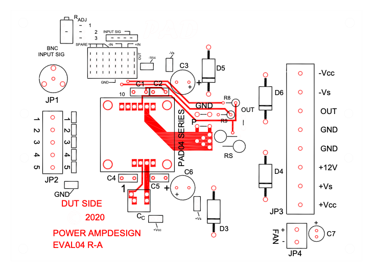
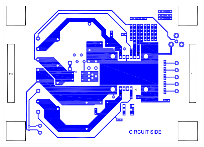
1. Notice that the printed circuit board (PCB) is labeled on one side as the “DUT SIDE” and the other side as “CIRCUIT” side.
2. D3 and D5 are transient voltage suppressor diodes and are not supplied since the type (breakdown voltage) varies with the application. They are not necessary for every application. They are most commonly used in application circuits where kickback from the load may force the supply voltage above the limits of the amplifier.
3. The evaluation kit PCB can be mounted in several ways. Option 1- Chassis mount. Use #6 standoffs and screws (not supplied) attached to the PCB at the four corners of the PCB.
Option 2- Bench-top mount. Use the rubber bumpers supplied. These are “stick-on” components. Remove the release paper from each bumper and apply the bumper to the square outlines on the “CIRCUIT SIDE” of the PCB.
Option 3- DIN rail mount. The PCB can be mounted to a 35mm DIN rail. For mounting the PCB to a DIN rail press the adaptors into the PCB in the holes at the edges of the PCB at locations 1 and 2 from the “CIRCUIT SIDE” of the PCB. Make sure that the plastic tines have fully spread out on the “DUT SIDE” of the PCB.
4. One or two resistors in parallel can be installed at Rs for use as a sense resistor for a Howland current pump. Otherwise install a jumper wire at Rs. R8 and R9 can also be installed to facilitate the Howland application. See the schematic of the EVAL04 board.
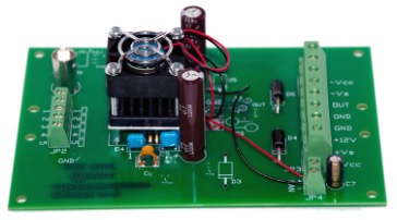
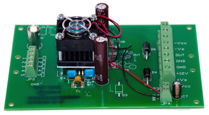
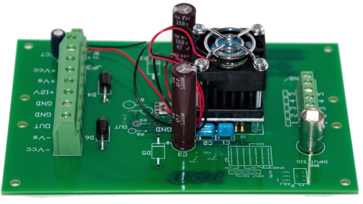
Assembled EVAL04 with amplifier installed.
5. Remove the 4 hex nuts from the mounting spacers of the amplifier.
6. Align the 4 studs of the mounting spacers with the mounting holes in the PCB. Be sure that the amplifier’s pin 1 aligns with pin 1 on the PCB. Slowly lower the amplifier into the PCB, making sure that the pins of the amplifier and the cage-jacks mate. Push the amplifier into the PCB until the mounting spacers meet the PCB.
7. Fasten the amplifier to the PCB with the 4 hex nuts previously removed. Do not over-tighten the nuts as this may strip the mounting studs. The provided plastic nut starter can assist you here.
8. If necessary, strip 1/8” of insulation from the wires connected to the fan. Twist and tin the wire ends. Insert the red wire into JP4 (FAN) at “+” and the black or blue wire into JP4 at “─”.
9. Use the bread-boarding area to add the external components necessary to program the amplifier gain and other circuit requirements to evaluate your application circuit. You can use the evaluation kit schematic and PCB views to map out your circuit.
10. Remember that the amplifier must be compensated to operate correctly. See the amplifier datasheet on Page 4, under PHASE COMPENSATION. The selected phase compensation capacitor will be installed at “CC” on the evaluation kit PCB. A 150pF capacitor has already been installed in your kit. Another
value may better suit your application. Remove and replace the capacitor as necessary for your application. 33pF and 100pF capacitors are also included with the kit. CC must be rated for the full supply voltage +Vs to -Vs is required. A temperature stable type capacitor is required—an X7R ceramic, for example, or an NPO type.
11. The evaluation kit assembly is complete. Be sure you have read and followed all the assembly steps. Inspect the circuit board for solder shorts or poor solder joints. An illuminated magnifier is helpful. It is best to remove the solder flux at the solder joints where components were added. Be sure to check that you have added either a resistor(s) or a jumper at Rs. Otherwise, the amplifier output will have no path to the output terminal block. Also, normally -Vs and -Vcc are tied together at JP3 as well as +Vs and +Vcc. Double check that you have made these connections. If you plan to drive an ink jet print head you may see AN46 on the web site.
12. Before applying power to your circuit set the power supply for ±20V and set the power supply current limit to approximately 100mA. Use little or no load at first. Apply an input signal and check the output with an oscilloscope to verify proper functionality. This step can prevent damaging the amplifier or the circuit board should there be some mistake in assembly.
Note that the amplifier is purchased separately.
CIRCUIT DIAGRAM
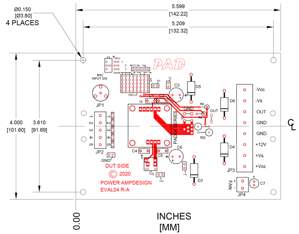
PCB VIEWS
TOP VIEW
BOTTOM VIEW
ASSEMBLED KIT
ASSEMBLED EVAL01 WITH AMPLIFIER MOUNTED
DIMENSIONAL INFORMATION