PAD0159 – Rev C
KEY FEATURES
- LOW COST
- POWER BOOSTER FOR PAD157
- HIGH OUTPUT CURRENT – 40A
- 500 WATT OUTPUT CAPABILITY
- 275 WATT DISSIPATION CAPABILITY
- INTEGRATED HEAT SINK AND FAN
- RoHS COMPLIANT DESIGN
APPLICATIONS
- LINEAR MOTOR DRIVE
- INDUSTRIAL AUDIO
- SEMICONDUCTOR TESTING
- VIBRATION CANCELLATION
- PROGRAMMABLE POWER SUPPLY
DESCRIPTION
The PAD159 power booster is designed to extend the output stage capabilities of the PAD157 RRIO amplifier in both power dissipation and output current. Together with the PAD157 the combined amplifier can provide an output current of 70A and provide a total internal power dissipation of 500W. The PAD157 operates as a “master” and the PAD159 follows its output command as a “slave”. The PAD157-PAD159 combination eliminates the need to use the parallel op amps application to increase output current and power dissipation and avoids the pitfalls of this application as applied to power op amps. For example, no balancing resistors are required and start-up problems are eliminated as well as stability issues in the slave unit. The PAD159 simply follows the output current command of the PAD157. The PAD159 is a dedicated design not intended to be used with any other amplifier model. No BeO is used in the PAD159.
A NEW CONCEPT
A critical task in any power amplifier application is cooling the amplifier. Until now component amplifier manufacturers often treated this task as an after-thought, left for the user to figure out. At Power Amp Design the best heat sink and fan is chosen at the start and becomes an integral part of the overall amplifier design. The result is the most compact and volumetric efficient design combination at the lowest cost. In addition, this integrated solution concept offers an achievable real-world power dissipation rating, not the ideal rating usually cited when the amplifier case is somehow kept at 25oC. The user no longer needs to specify, procure or assemble separate components.
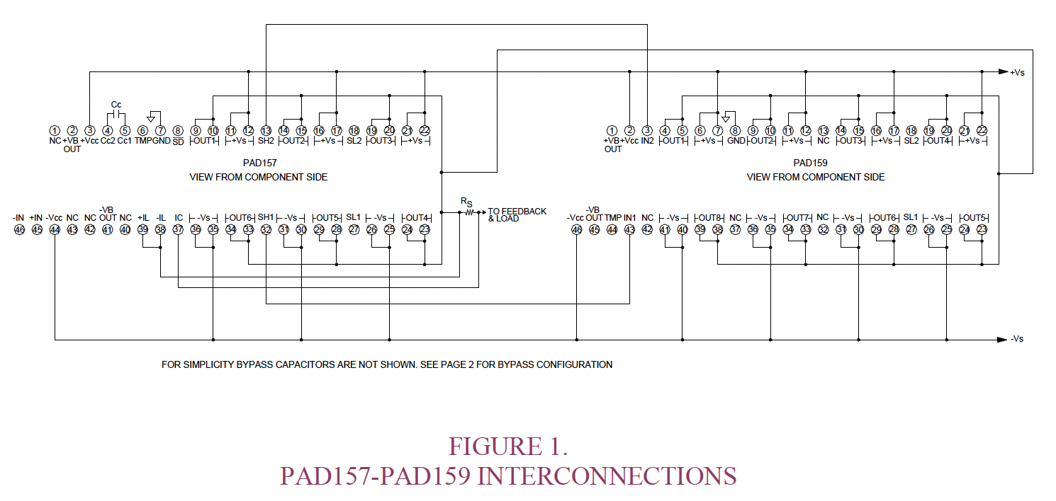
CIRCUIT & CONNECTIONS
EQUIVALENT CIRCUIT
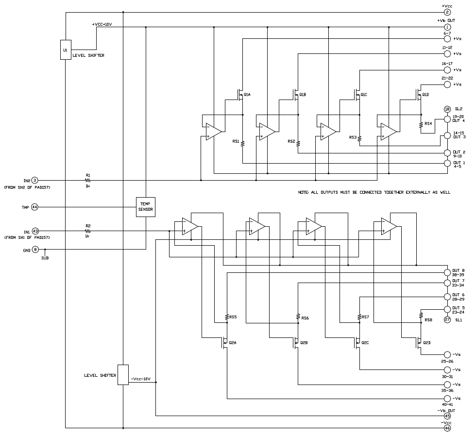
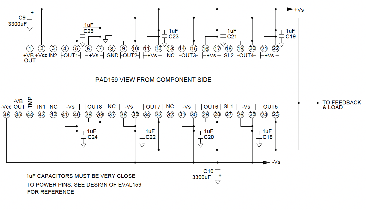
AMPLIFIER PINOUT & CONNECTIONS
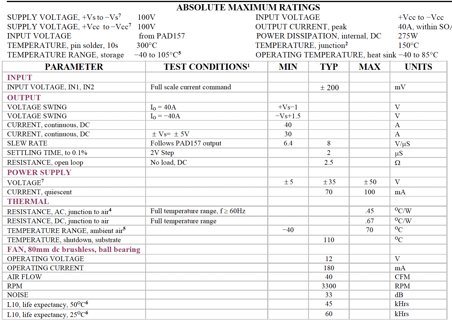
ABSOLUTE MAXIMUM RATINGS
NOTES
1. Unless otherwise noted: TC=25OC DC input specifications are value given, power supply voltage is typical rating.
2. Derate internal power dissipation to achieve high MTBF.
4. Rating applies if the output current alternates between both output transistors at a rate faster than 60Hz.
5. Limited by fan characteristics. During operation, even though the heat sink may be at 85OC or more the fan will be at a lower temperature.
6. L10 refers to the time it takes for 10% of a population of fans to fail. Lower ambient temperature increase fan life.
7. +Vs, +Vcc must be connected together. –Vs, –Vcc must be connected together.
POWER BOOSTER FUNCTION
The PAD159 power booster amplifier is designed to extend the output power, output current and internal power dissipation of the PAD157 power operational amplifier. The current sense outputs from the PAD157 are fed to the inputs of the PAD159 to command the PAD159 output current. In the application the PAD157 is configured as if it were the only amplifier, so connections for gain, current limit and shutdown are the same for the PAD157-PAD159 combination as they would be for the PAD157 alone. In the combination of the PAD157 and PAD159, the PAD157 controls the output voltage of both amplifiers while the PAD159 follows the output current of the PAD157. The two amplifiers together function as one power operational amplifier with greater capability than the PAD157 alone. The PAD159 is a dedicated design not intended to work with any other amplifier model. Required interconnections of the two amplifiers are shown in Figure 1 on page 6.
GENERAL SPECIFICATIONS
Since it is constructed from the same components as the PAD157, the PAD159 is expected to provide the same bandwidth, slew rate and output voltage swing as the PAD157 it is connected to. The PAD159 has its own separate substrate temperature sensor, necessary to drive its own external fan controller (PAD131). The PAD159 also has its own charge pump power supply and so its +VB OUT and -VB OUT pins should not be connected to the similar pins of the PAD157. When the PAD157 goes into shutdown, either from an over-temperature condition or an external command, the PAD159 shuts down also since the PAD159 follows the output current command of the PAD157. There is no separate shutdown command for the PAD159.
CURRENT LIMIT
Since the PAD159 follows the output current command of the PAD157 any current limit condition of the PAD157 is reflected in the PAD159 as well. For example, if the current limit set point is, say, 10A, that 10 amps is shared between the PAD157 and PAD159. When the PAD157 goes into current limit so then does the PAD159 as well. See the data sheet of the PAD157 for the details of the current limit function of the PAD157.
COOLING FAN
The PAD159 relies on its fan for proper cooling of the amplifier. Make sure that air flow to the fan and away from the heat sink remains unobstructed. To eliminate electrical noise created by the cooling fan we recommend a 47µF capacitor placed directly at the point where the fan wires connect to the PCB. See application note AN-24 for further details.
The operating voltages of the PAD04 are potentially deadly. When developing an application circuit, it is wise to begin with power supply voltages as low as possible while checking for circuit functionality. Increase supply voltages slowly as confidence in the application circuit increases. Always use a “hands-off” method whereby test equipment probes are attached only when power is off.
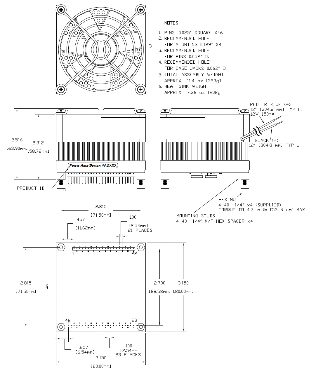
MOUNTING THE AMPLIFIER
The amplifier is supplied with four 4-40 M/F hex spacers at the four corners of the amplifier. Since the male threaded ends of the spacers extend beyond the amplifier pins the spacers provide a convenient alignment tool to guide the insertion of the amplifier pins into the circuit board. Once the amplifier is seated secure the module with the provided 4-40 nuts and torque to 4.7 in lb [53 N cm] max. See “Dimensional Information” for a detailed drawing. It is recommended that the heat sink be grounded to the system ground. This can easily be done by providing a grounded circuit board pad around any of the holes for the mounting studs.
TEMPERATURE REPORTING
An analog output voltage is provided (pin 44, TMP) relative to ground and proportional to the temperature in degrees C. The slope is approximately -10.82mV/oC. The output voltage follows the equation:
T = (2.127 ─ V) (92.42)
Where V is the TMP output voltage and T is the substrate temperature in degrees C.
Note that the PAD157 and PAD159 may operate at somewhat different temperatures. The total power dissipation of the PAD159 is larger due to its 4 parallel output transistors whereas the PAD157 has only 3 parallel output transistors. Even so, the PAD159 spreads out the power dissipation over a larger area of the heat sink and the temperatures of the two amplifiers will be similar though not exactly the same. The two amplifiers will share the total output current in a ratio of 4:3.
THERMAL SHUTDOWN
The temperature monitoring circuit of the PAD157 automatically turns off the output transistors when the substrate temperature reaches 110oC. When the substrate cools down 10oC the output is enabled once again. The thermal shutdown feature is activated either by amplifier overloads or a failure of the fan circuit. The PAD159 follows the PAD157 commands and so there is no separate thermal shutdown function in the PAD159.
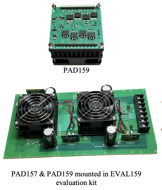
EVALUATION KIT EVAL159
An evaluation kit, EVAL159, is available with sockets for both the PAD157 and PAD159 and all the interconnections already made on the board as well as the main components necessary to build the application circuit before going to production. Good layout technique is also demonstrated in the board design. See the data sheet for the EVAL159 design details. Note the 4 copper layer design.
CONNECTING ADDITIONAL PAD159s
More than one PAD159 many be connected to a PAD157. Additional PAD159s may be connected by tying the PAD157’s SH1 to the IN1 pins of all PAD159s and the PAD157’s SH2 to the IN2 pins of all PAD159s.
MOTHER-BOARD LAYOUT CONSIDERATIONS
The EVAL159 evaluation kit board demonstrates good layout technique for the PAD157-PAD159 combination. Since the combination of these two amplifier models can provide a very large output current, the board uses a four-layer design. Large traces for power supply are doubled-up, where traces for these connections appear on two or more layers and are thus in parallel for lower resistance. In the EVAL159 all four layers are 2oz CU. On the top layer all of the outputs of both amplifiers are tied together. The pcb pattern connecting all the outputs on the top layer are copied on two additional inner layers and thus are in parallel for low resistance to handle the output current which can be very large and also because it is important that the output connections between the amplifiers is a very low resistance. It is very important that Separate electrolytic by-pass capacitors are provided for each amplifier and 1uF ceramic capacitors are placed very close to all power supply pins. Bypassing is critical. Follow the design technique of the EVAL159 for reference. See the EVAL159 data sheet for views of the four layers.
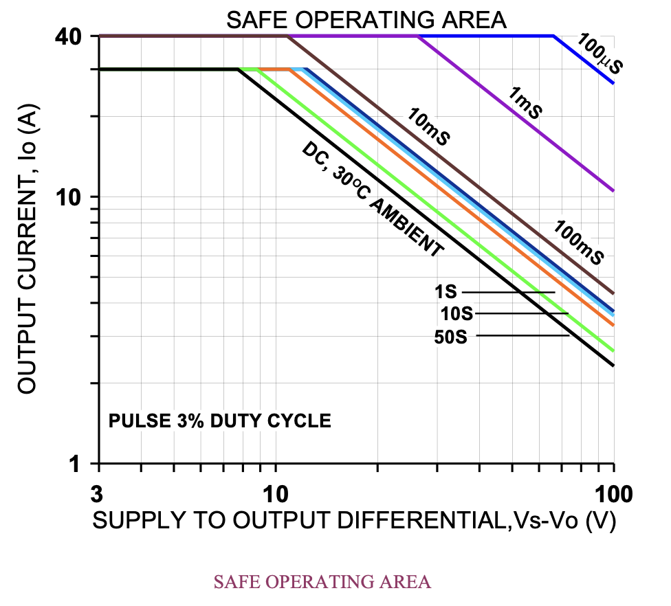
SAFE OPERATING AREA
DIMENSIONAL INFORMATION