PAD541 – Rev E
KEY FEATURES
- LOW COST
- HIGH VOLTAGE – 100 VOLTS
- HIGH OUTPUT CURRENT – 5 AMPS
- 50 WATT DISSIPATION CAPABILITY
- 100 WATT OUTPUT CAPABILITY
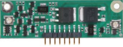
- 0.63” HEIGHT SIP DESIGN
APPLICATIONS
- LINEAR MOTOR DRIVE
- HIGH VOLTAGE INSTRUMENTATION
- SEMICONDUCTOR TESTING
- TEST EQUIPMENT
DESCRIPTION
The PAD541 compact operational amplifier is constructed with surface mount components to provide a cost effective solution for many industrial applications. The SIP design is only 0.63” high and provides clearance for those applications where circuit boards are mounted side by side in a card cage. The PAD541 exceeds the performance of monolithic amplifiers while having a similar height dimension. User selectable external compensation tailors the amplifier’s response to the application requirements. Programmable current limit is built-in. The amplifier circuitry is built on a thermally conductive but electrically insulating substrate. No BeO is used in the PAD541. The resulting module is a small, high performance simple solution for many industrial applications.
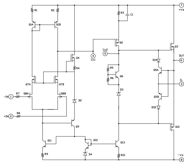
EQUIVALENT CIRCUIT
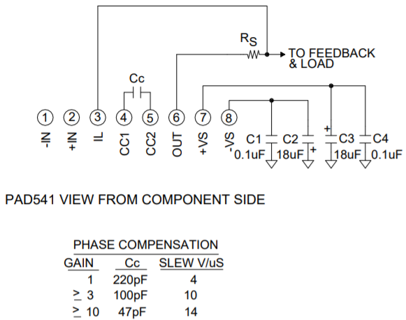
PINOUT & CONNECTIONS
ABSOLUTE MAXIMUM RATINGS SPECIFICATIONS
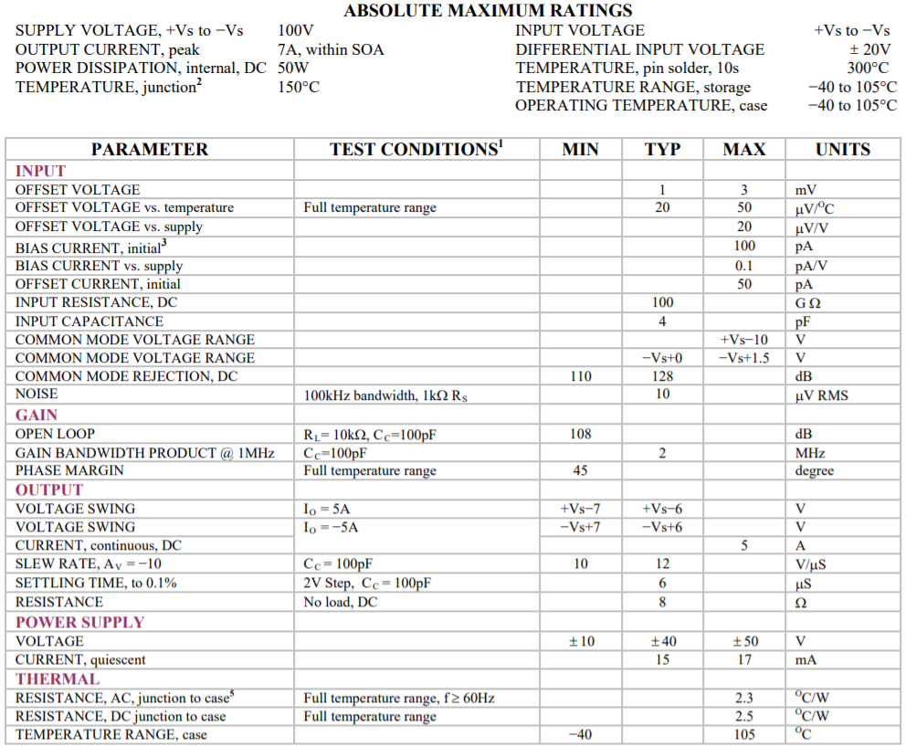
NOTES:
- Unless otherwise noted: TC = 25OC, compensation Cc = 470pF, DC input specifications are ± value given, power supply voltage is typical rating.
- Derate internal power dissipation to achieve high MTBF.
- Doubles for every 10OC of case temperature increase.
- +Vs and −Vs denote the positive and negative supply voltages.
- Rating applies if the output current alternates between both output transistors at a rate faster than 60Hz.
OPERATING CONSIDERATIONS
SAFETY FIRST
The operating voltages of the PAD541 are potentially deadly. When developing an application circuit it is wise to begin with power supply voltages as low as possible while checking for circuit functionality. Increase supply voltages slowly as confidence in the application circuit increases. Always use a “hands off” method whereby test equipment probes are attached only when power is off
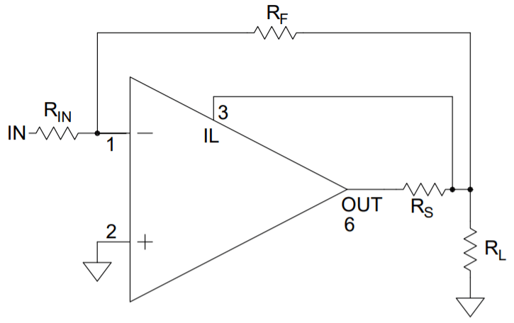
CURRENT LIMIT
The current limiting function of the PAD541 is externally programmable. See Figure 1. The sense voltage for current limit is 0.65V. Thus:
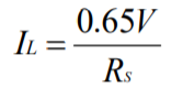
Where IL is the value of the limited current and RS is the value of the current limit sense resistor.
In addition, the sense voltage has a temperature coefficient approximately equal to –2.2mV/℃ case temperature.
MOUNTING THE AMPLIFIER
In most applications the amplifier must be attached to a heat sink. Spread a thin and even coat of heat sink grease across the back of the PAD541 and also the heat sink where the amplifier is to be mounted. Push the amplifier into the heat sink grease on the heat sink while slightly twisting the amplifier back and forth a few times to bed the amplifier into the heat sink grease. On the final twist align the mounting holes of the amplifier with the mounting holes in the heat sink and finish the mounting using 2-56 screw and a #2 stainless steel internal tooth lock washer. The lock washer helps to electrically connect the substrate to the heat sink (that should be grounded). Torque the screws to 2.2 in pound (0.248 N meter) maximum. Do not rely on the screw pressure to squeeze out any excess heat sink grease as this will likely only bend the substrate at the corners. See “Dimensional Information” for a detailed drawing. It is recommended that the heat sink be grounded to the system ground.
PHASE COMPENSATION
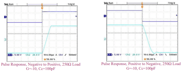
The PAD541 must be phase compensated. The compensation capacitor, CC, is connected between pins 4 and 5. The compensation capacitor must be an NPO type capacitor rated for the full supply voltage (100V). On page 2, under Amplifier Pinout and Connections, you will find a table that gives recommended compensation capacitance value for various circuit gains and the resulting slew rate for each capacitor value. Consult also the small signal response and phase response plots for the selected compensation value in the Typical Performance Graphs section. A compensation capacitor less than 47pF is not recommended.
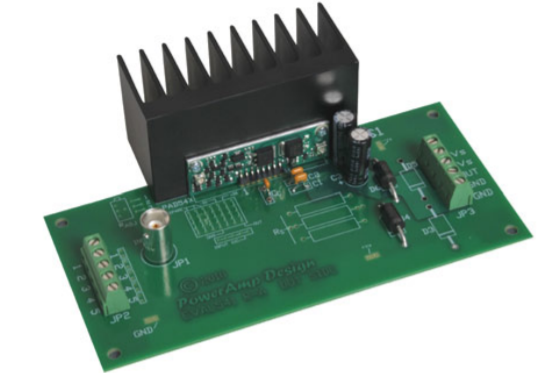
EVALUATION KIT
An EVAL541 evaluation kit is available that is helpful in developing your application circuit. The kit includes a heat sink, input and output jacks, bypass capacitors and a selection of current limiting resistor values as well as a bread-boarding area to configure the amplifier according to your application circuit requirements. The kit helps you rapidly build and evaluate your application circuit without having to construct your own board and research and purchase suitable components. The PCB pre-wires critical connections for power supply bypassing and ground connections thus minimizing mistakes in wiring and optimizing circuit layout.
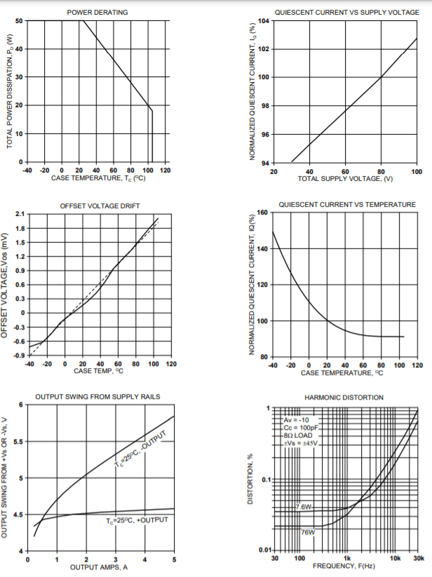
TYPICAL PERFORMANCE GRAPHS
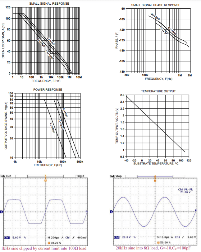
ERFORMANCE GRAPHS CONTINUED
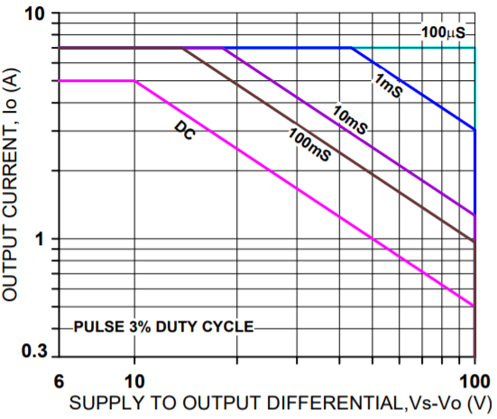
SAFE OPERATING AREA
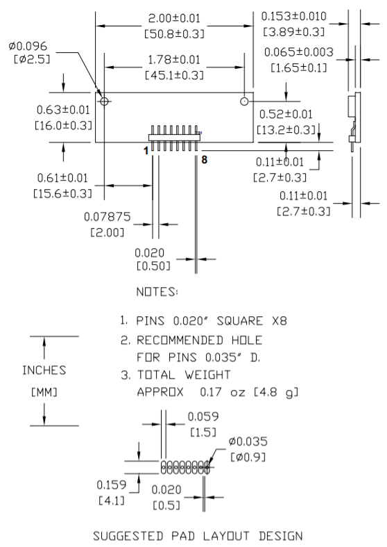
DIMENSIONAL INFORMATION