PAD189A – Rev B
KEY FEATURES
- LOW COST
- HIGH VOLTAGE – 1050 VOLTS
- HIGH OUTPUT CURRENT – 1.5A
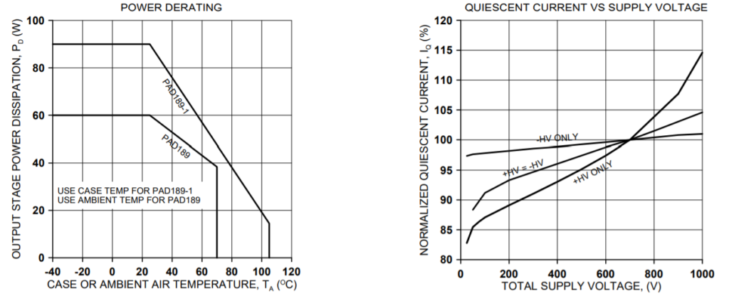
- 60 WATT DISSIPATION CAPABILITY
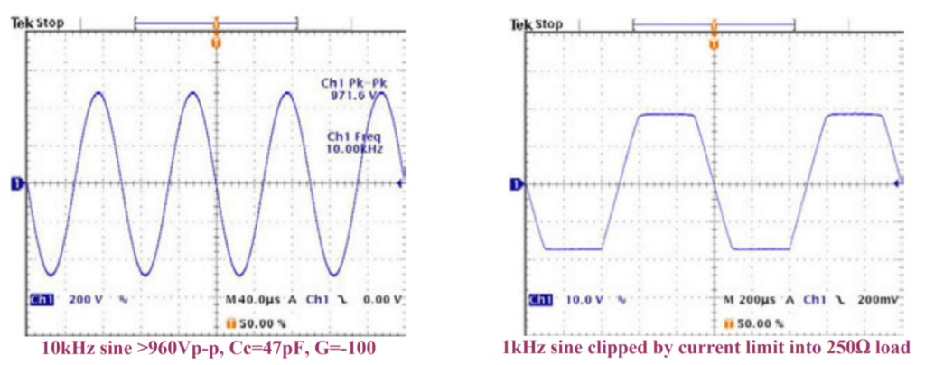
- 10kHz POWER BANDWIDTH –1000V p-p
- INTEGRATED HEAT SINK AND FAN
- CONFORMAL COATED CIRCUIT
APPLICATIONS
- PIEZO TRANSDUCER DRIVE
- HIGH VOLTAGE INSTRUMENTATION
- SEMICONDUCTOR TESTING
DESCRIPTION
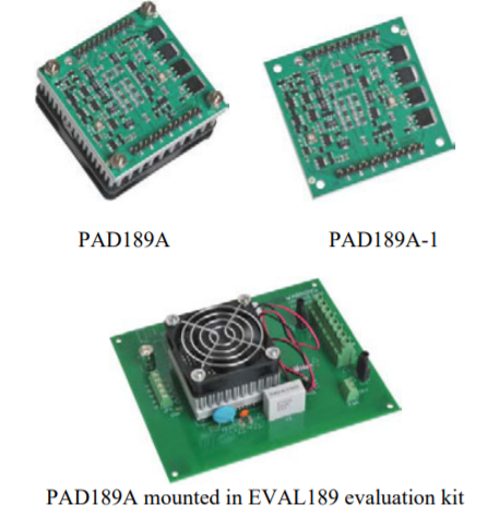
The PAD189A high voltage operational amplifier is constructed with surface mount components to provide a cost effective solution for many industrial applications. With a footprint only 5.6in2 the PAD189A offers outstanding performance that rivals much more expensive hybrid component amplifiers or rack-mount amplifiers. An externally programmable current limit can be set with a single resistor. User selectable external compensation tailors the amplifier’s response to the application requirements. The PAD189A circuitry is built on a thermally conductive but electrically insulating substrate mounted to an integral heat sink and fan assembly. The resulting module is a small, high performance simple solution for many industrial applications. The PAD189A-1 is also available without the heat sink and fan for custom applications. The circuit is conformal coated for additional safety and reliability. See “CONFORMAL COATING” paragraph on page 5.
A NEW CONCEPT
A critical task in any power amplifier application is cooling the amplifier. Until now component amplifier manufacturers often treated this task as an after-thought, left for the user to figure out. At Power Amp Design the best heat sink and fan combination is chosen at the start and becomes an integral part of the overall amplifier design. The result is the most compact and volumetric efficient design combination at the lowest cost. In addition, this integrated solution concept offers an achievable real-world power dissipation rating, not the ideal rating usually cited when the amplifier case is somehow kept at 25℃. The user no longer needs to specify, procure or assemble separate components.
CIRCUIT & CONNECTIONS
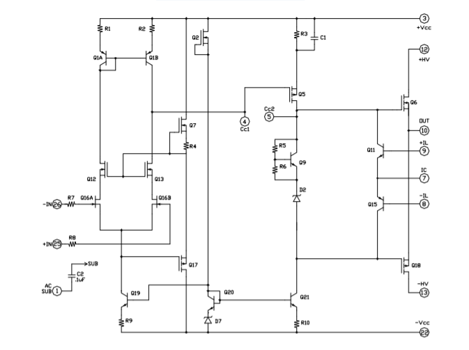
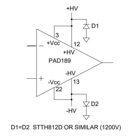
EQUIVALENT CIRCUIT
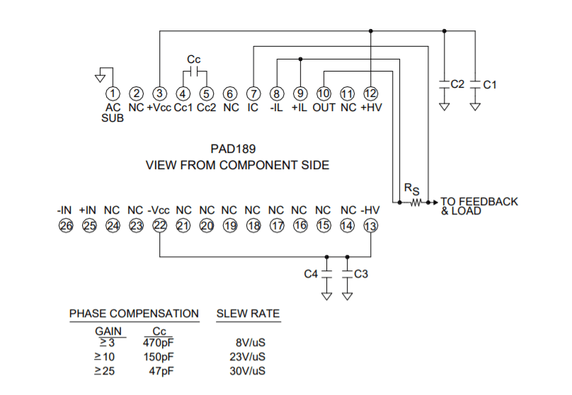
PINOUT & CONNECTIONS
ABSOLUTE MAXIMUM RATINGS SPECIFICATIONS
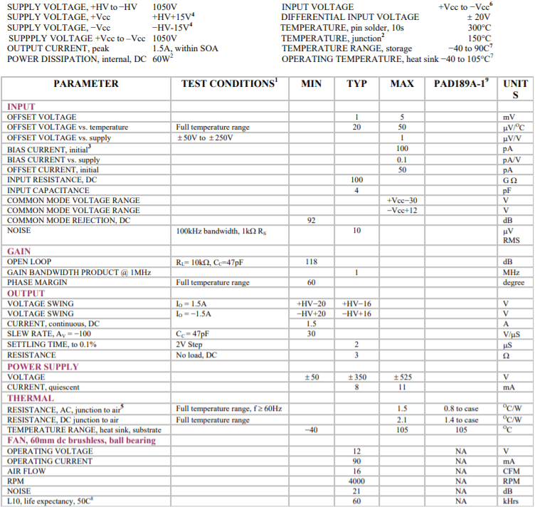
NOTES:
- Circuit is conformal coated. See paragraph “Conformal Coating” on page 5.
- Unless otherwise noted: TC=25℃, compensation Cc=220pF, DC input specifications are ± value given, power supply voltage is typical rating.
- Derate internal power dissipation to achieve high MTBF.
- Doubles for every 10℃ of case temperature increase.
- +HV and −HV denote the positive and negative supply voltages to the output stage. +Vcc and −Vcc denote the positive and negative supply voltages to
the input stages. - Rating applies if the output current alternates between both output transistors at a rate faster than 60Hz.
- Power supply voltages +Vcc and −Vcc must not be less than +HV and −HV respectively. Total voltage +Vcc to –Vcc not to exceed 1000V.
- Limited by fan storage characteristics. During operation, even though the case may be at 85OC the fan will be at a lower temperature.
- L10 refers to the time it takes for 10% of a population of fans to fail.
- Specifications for the PAD189A-1 are the same as for the PAD189A except as shown in this column.
OPERATING CONSIDERATIONS
SAFETY FIRST
Remember at all times that the operating voltages of the PAD189A are potentially deadly. When developing an application circuit it is wise to begin with power supply voltages as low as possible while checking for circuit functionality. Increase supply voltages slowly as confidence in the application circuit increases. Always use a “hands off” method whereby test equipment probes are attached only when power is off.
COOLING FAN
The PAD189A relies on its fan for proper cooling of the amplifier. Make sure that air flow to the fan and away from the heat sink remains unobstructed. The cooling method used is impingement cooling, which means that cool air is pushed into the heat sink and warm air is exhausted through the spaces between the heat sink fins. To eliminate electrical noise created by the cooling fan we recommend a 47µF capacitor placed directly at the point where the fan wires connect to the PCB. See application note AN-24 for further details.
MOUNTING THE PAD189A AMPLIFIER
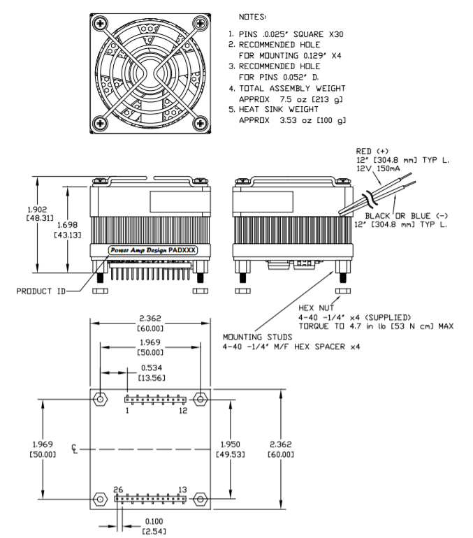
The amplifier is supplied with four 4-40 M/F hex spacers at the four corner of the amplifier. Since the male threaded ends of the spacers extend beyond the amplifier pins the spacers provide a convenient alignment tool to guide the insertion of the amplifier pins into the circuit board. Once the amplifier is seated, secure the module with the provided 4-40 nuts and torque to 4.7 in lb [53 N cm] max. See “Dimensional Information” for a detailed drawing. It is recommended that the heat sink be grounded to the system ground. This can easily be done by providing a grounded circuit board pad around any of the holes for the mounting studs.
MOUNTING THE PAD189A-1 AMPLIFIER
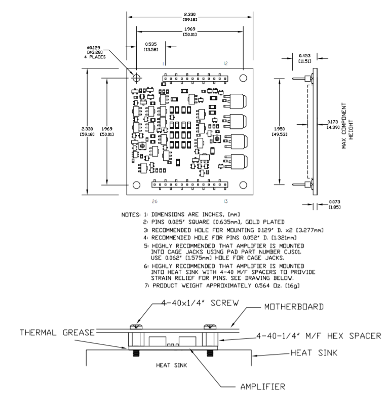
In most applications the amplifier must be attached to a heat sink. Spread a thin and even coat of heat sink grease across the back of the PAD189A-1 and also the heat sink where the amplifier is to be mounted. Push the amplifier into the heat sink grease on the heat sink while slightly twisting the amplifier back and forth a few times to bed the amplifier into the heat sink grease. On the final twist align the mounting holes of the amplifier with the mounting holes in the heat sink and finish the mounting using 4-40 hex male-female spacers and torque to 4.7 in oz [3.8 N cm] max. Mount the amplifier to the mother board with 4-40 X 1/4” screws. See Dimensional Information for additional recommendations.
EXTERNAL CIRCUIT COMPONENTS
The output of the PAD189A can swing up to +/- 500V and this may stress or destroy external components that are often not seriously considered when developing circuits with small signal op amps. For example, it is often overlooked that the usual voltage rating for metal film resistors is only 200V and that application circuits using the PAD189A may place up to 1000V across the feedback resistor. High voltage rated resistors may be purchased for the feedback circuit or, alternately, several ordinary resistors may be placed in series to obtain the proper voltage rating. We recommend five resistors in series for the feedback resistor. The compensation capacitor CC is a NPO type and is rated for 1000V. The voltage rating of the connecting wire and PCB spacing between pads and connecting traces needs to be considered as well. See application note AN-16 for details.
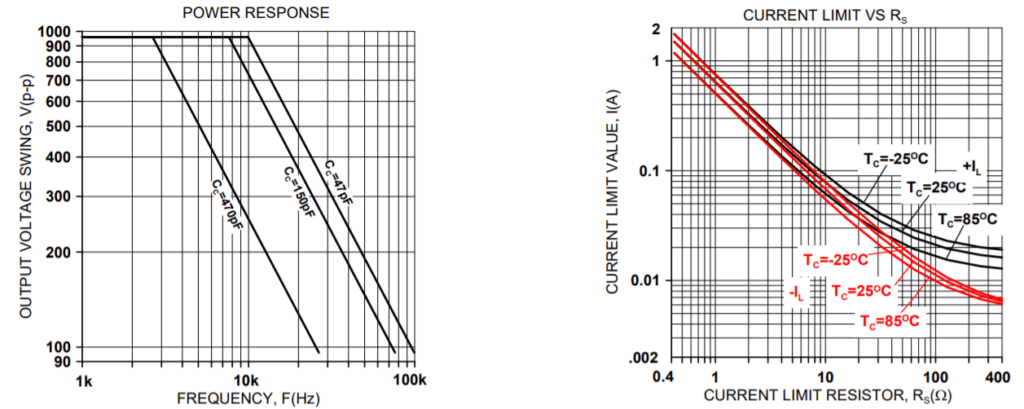
CURRENT LIMIT
Current limit can be programmed by attaching a suitable value resistor as shown in Figure 1. The value of the limited current can be approximately calculated by:
IL=.65/RS
Where IL is the value of the limited current and RS is the value of the current sense resistor. It is important that the type of resistor chosen for RS be non-inductive. A wirewound resistor is not a good choice even if it rated as “noninductive” since it will exhibit significant inductance at some frequency. A better choice is a type of resistor that is more inherently non-inductive such as a powdered metal resistor or a thick film resistor. The power dissipation rating of the sense resistor should not to be forgotten. The current limit circuitry works by diverting the stage currents of the amplifier into the output circuit (about 5mA) and this introduces an error term compared to the approximate equation given above. As the current limit value is reduced the proportion of the error term increases. The practical range of current limit is from 20mA to 1.5A. The current limit decreases 2.2mV/℃ with increasing temperature since the sense voltage for calculating the current limit is the emitter-base circuit of a bipolar transistor.
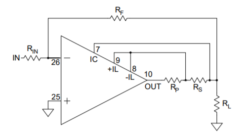
Current Limit
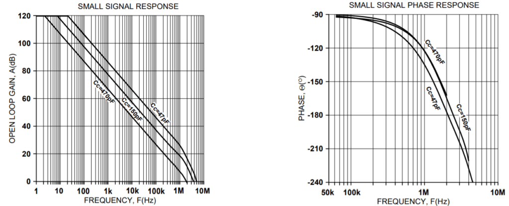
PHASE COMPENSATION
The PAD189A must be phase compensated to operate correctly. The compensation capacitor, CC, is connected
between pins 4 and 5. On page 7, Typical Performance Graphs, you will find plots for small signal response and phase response using various compensation values. The compensation capacitor must be an NPO type capacitor rated for the full supply voltage (1000V). On page 2, under Amplifier Pinout and Connections, a table gives recommended compensation capacitance values for various gains and the resulting slew rate for each capacitor value.
INPUT PROTECTION
In applications where the input differential voltage may be exceeded (dc or transient) it is important to add differential input voltage protection. See Figure 2.
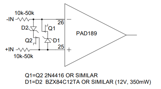
Input differential voltage protection
It is also important that the power supply connections to the PAD189A not be open. If for example, the negative supply connection were to open (perhaps a faulty connection) the internal circuitry of the amplifier will bootstrap the amplifier to the positive supply through the feedback gain-setting resistor. When the +IN is grounded the input circuit is clamped to ground while the output of the amplifier will float to the positive supply voltage via the boot-strapping effect. The input differential voltage of the amplifier will be exceeded destroying the input stage. This is one good reason to protect the input as shown in Figure 2. But it is also a good reason to clamp the power supply pins as shown in Figure 3.
CONFORMAL COATING
The circuit of the PAD189A is covered by a silicone conformal coating for extra protection against internal arcing and environmental considerations such as humidity. The conformal coating is soft and may be damaged by rough handling. It is therefore recommended that the circuit be handled only by the edges of the substrate to avoid disturbing the coating. The PAD189A is only rated for normal environmental conditions of atmospheric pressure, humidity and temperature usually found in a laboratory or production floor.
Power supply clamps
TYPICAL PERFORMANCE GRAPHS
SAFE OPERATING AREA
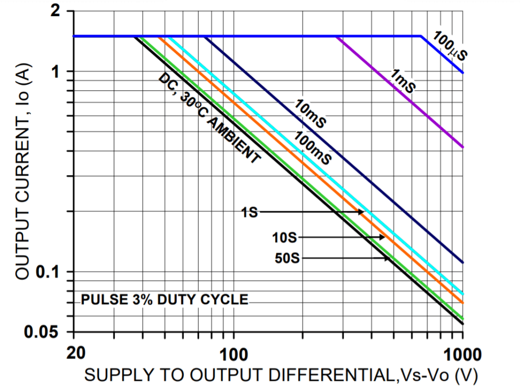
The safe operating area (SOA) of a power amplifier is its single most important specification. The SOA graph presented above serves as a first approximation to help you decide if the PAD189A will meet the demands of your application. But a more accurate determination can be reached by making use of the PAD Power™ spreadsheet which can be found in the Power Amp Design website under Design Spreadsheet tab. While the graph above adequately shows DC SOA and some pulse information it does not take into account ambient temperatures higher than 30℃, AC sine, phase or non-symmetric conditions that often appear in real-world applications. The PAD Power™ spreadsheet takes all of these effects into account.
DIMENSIONAL INFORMATION