Downloads
Datasheet
PAD150 – Rev C
KEY FEATURES
- LOW COST
- SMALL SIZE 40 X 45mm
- HIGH VOLTAGE – 100 VOLTS
- HIGH OUTPUT CURRENT – 20A PEAK
- 125 WATT DISSIPATION CAPABILITY
- 200V/µS SLEW RATE
- RoHS COMPLIANT
APPLICATIONS
- INDUSTRIAL INK JET PRINT HEADS
- HIGH VOLTAGE INSTRUMENTATION
- PIEZO TRANSDUCER DRIVE
DESCRIPTION
The PAD150 compact high voltage op amp is constructed with surface mount components to provide a cost effective solution for many industrial applications such as an ink jet print head driver. With a footprint only 40 X 45mm the PAD150 offers outstanding performance that rivals more expensive hybrid components. User selectable external compensation tailors the amplifier’s response to the application requirements. The PAD150 is built on a thermally conductive but electrically insulating substrate. No BeO is used in the PAD150.
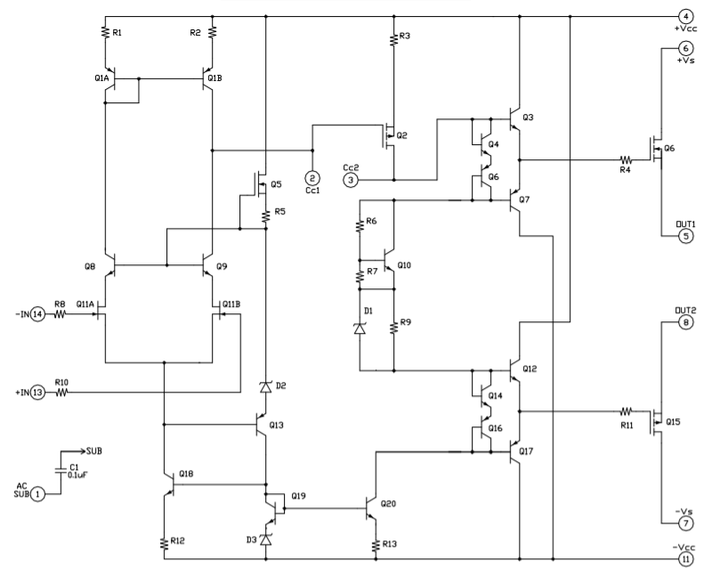
CIRCUIT & CONNECTIONS
EQUIVALENT CIRCUIT
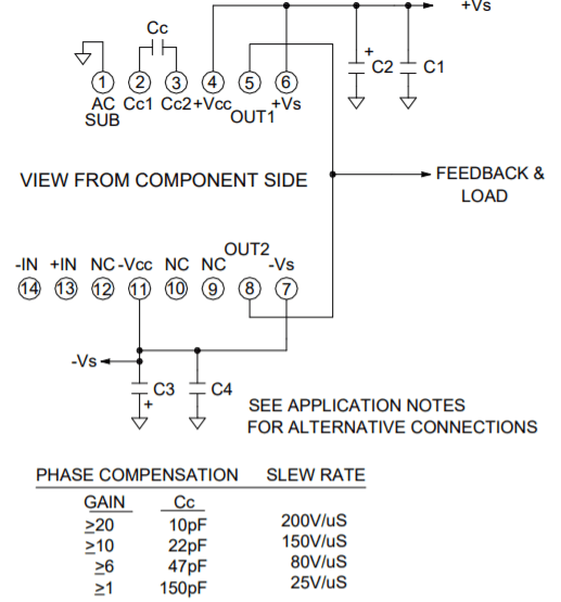
PINOUT & CONNECTIONS
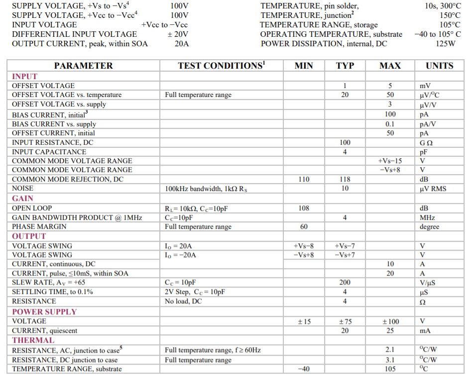
ABSOLUTE MAXIMUM RATINGS SPECIFICATIONS
NOTES:
- Unless otherwise noted: TC = 25℃, compensation Cc = 150pF, DC input specifications are ± value given, power supply voltage is typical rating.
- Derate internal power dissipation to achieve high MTBF.
- Doubles for every 10℃ of case temperature increase.
- +Vs and −Vs denote the positive and negative supply voltages to the output stage. +Vcc and –Vcc denote the positive and negative supply voltages to
the small signal stages. +Vcc and –Vcc may not be more than + and – 20V greater than +Vs and –Vs respectively. - Rating applies if the output current alternates between both output transistors at a rate faster than 60Hz.
- Power supply voltages +Vcc and −Vcc must not be less than +Vs and −Vs respectively. Total voltage +Vcc to −Vcc 100V maximum.
OPERATING CONSIDERATIONS
SAFETY FIRST
The operating voltages of the PAD150 are potentially deadly. When developing an application circuit it is wise to begin with power supply voltages as low as possible while checking for circuit functionality. Increase supply voltages slowly as confidence in the application circuit increases. Always use a “hands-off” method whereby test equipment probes are attached only when power is off.
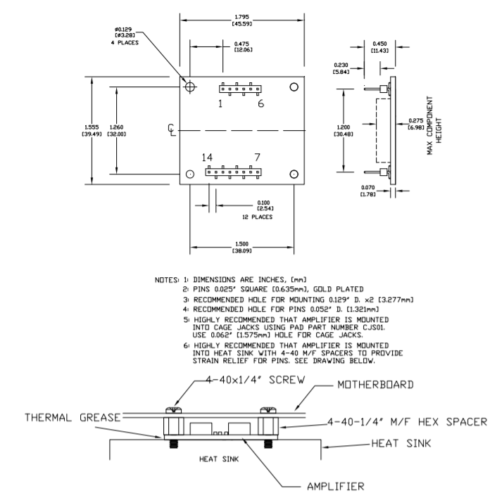
MOUNTING THE PAD150 AMPLIFIER
In most applications the amplifier must be attached to a heat sink. Spread a thin and even coat of heat sink grease across the back of the PAD150 and also the heat sink where the amplifier is to be mounted. Push the amplifier into the heat sink grease on the heat sink while slightly twisting the amplifier back and forth a few times to bed the amplifier into the heat sink grease. On the final twist align the mounting holes of the amplifier with the mounting holes in the heat sink and finish the mounting using 4-40 hex male-female spacers and torque to 4.7 in lb [53 N cm] max. Mount the amplifier to the mother board with 4-40 X 1/4” screws. See Dimensional Information for additional recommendations.
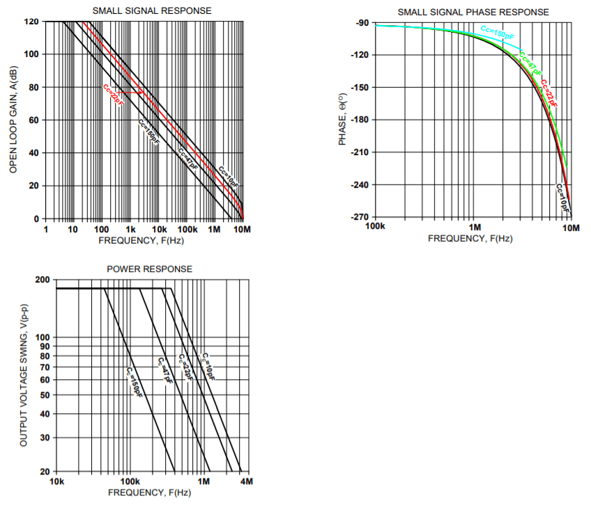
PHASE COMPENSATION
The PAD150 must be phase compensated. The compensation capacitor, CC, is connected between pins 2 and 3. The compensation capacitor must be an NPO type capacitor rated for the full supply voltage (100V). On page 2, under Amplifier Pinout and Connections, you will find a table that gives recommended compensation capacitance value for various circuit gains and the resulting slew rate for each capacitor value. Consult also the small signal response and phase response plots for the selected compensation value in the Typical Performance Graphs section. A compensation capacitor less than 10pF is not recommended.
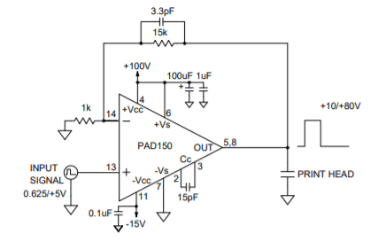
SINGLE HIGH-CURRENT SUPPLY OPERATION
It is often desirable to operate the PAD150 with a single high-current power supply as this reduces system cost. Figure 2 in the application circuits section shows one way to do this. However, in this case the input signal should be offset slightly to prevent the output from being driven to ground. When the output swings closer to ground than 10V the output transistor connected to the negative supply must recover from being over-driven. This causes a delay in the output going to a high condition. If the input signal is offset slightly so that the output is not driven to less than 10V this delay is avoided. The resulting output signal will then vary from 10V to 90V. For a circuit gain of +16 the required input signal then becomes 0.625V to 5.000V. For custom applications the PAD150 can be ordered with its offset voltage set to produce the same effect. This option is desirable in applications where adjusting the input signal is
difficult.
TYPICAL PERFORMANCE GRAPHS

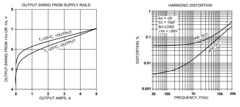
SAFE OPERATING AREA
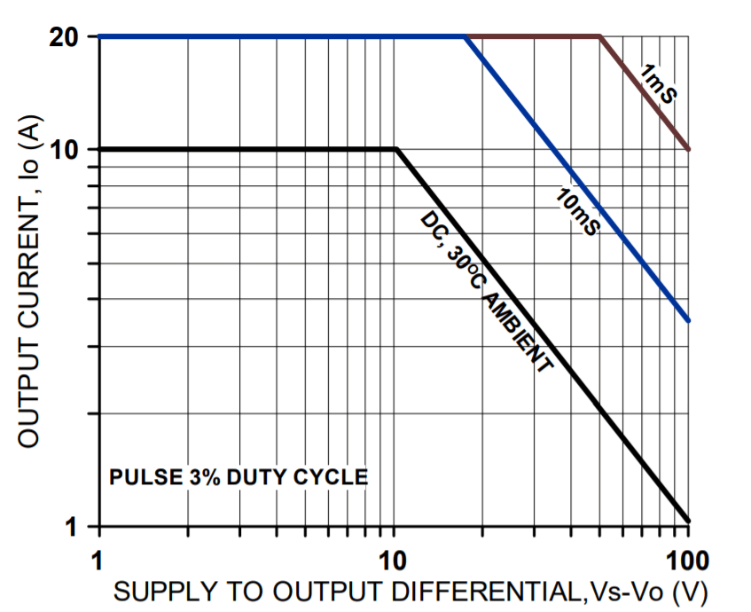
The safe operating area (SOA) of a power amplifier is its single most important specification. The SOA graph presented above serves as a first approximation to help you decide if the PAD150 will meet the demands of your application.
DIMENSIONAL INFORMATION
APPLICATION CIRCUITS
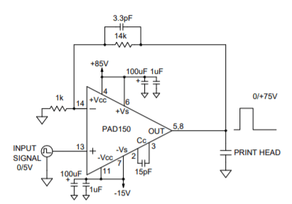
TYPICAL DUAL SUPPLY PRINT HEAD DRIVE CIRCUIT
SINGLE HIGH-CURRENT POWER SUPPLY PRINT HEAD DRIVE CIRCUIT