PAD138 – Rev C
KEY FEATURES
- LOW COST
- SMALL SIZE 40mm SQUARE
- HIGH VOLTAGE – 200 VOLTS
- HIGH OUTPUT CURRENT – 12A PEAK
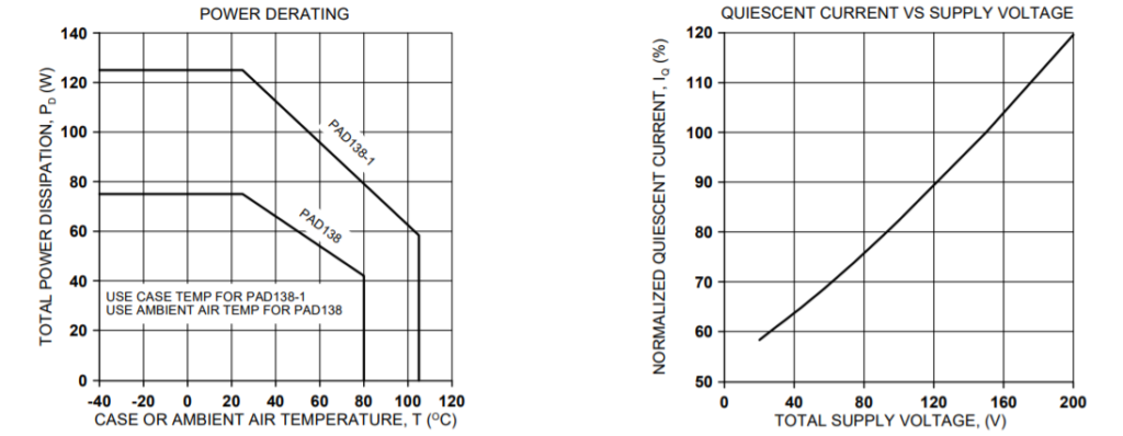
- 75 WATT DISSIPATION – PAD138
- 125 WATT DISSIPATION – PAD138-1
- 30V/µS SLEW RATE
- PROGRAMMABLE CURRENT LIMIT
- RoHS COMPLIANT
APPLICATIONS
- INDUSTRIAL INK JET PRINT HEADS
- HIGH VOLTAGE INSTRUMENTATION
- PIEZO TRANSDUCER DRIVE
- MOTOR DRIVE
DESCRIPTION
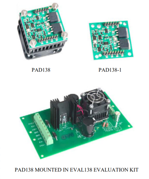
The PAD138 compact high voltage op amp is constructed with surface mount components to provide a cost effective solution for many industrial applications. With a footprint only 40mm square the PAD138 offers outstanding performance that rivals more expensive hybrid components. An integrated heat sink and fan cooling are included. User selectable external compensation tailors the amplifier’s response to the application requirements. The PAD138 is built on a thermally conductive but electrically insulating substrate. No BeO is used in the PAD138. For custom applications the PAD138-1 version of the amplifier is available without the integrated heat sink and fan. RoHS Compliant.
A NEW CONCEPT
A critical task in any power amplifier application is cooling the amplifier. Until now component amplifier manufacturers often treated this task as an after-thought, left for the user to figure out. At Power Amp Design the best heat sink and fan is chosen at the start and becomes an integral part of the overall amplifier design. The result is the most compact and volumetric efficient design combination at the lowest cost. In addition, this integrated solution concept offers an achievable real-world power dissipation rating, not the ideal rating usually cited when the amplifier case is somehow kept at 25℃. The user no longer needs to specify, procure or assemble separate components.
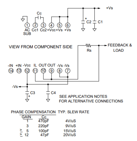
CIRCUIT & CONNECTIONS
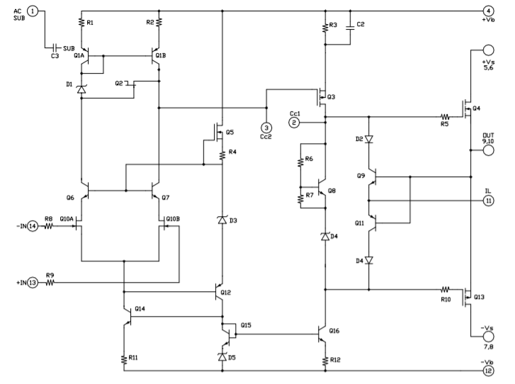
EQUIVALENT CIRCUIT
PINOUT & CONNECTIONS
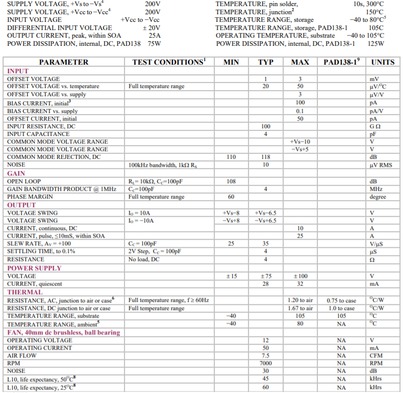
ABSOLUTE MAXIMUM RATINGS SPECIFICATIONS
NOTES:
- Unless otherwise noted: TC = 25℃, compensation Cc = 220pF, DC input specifications are ± value given, power supply voltage is typical rating.
- Derate internal power dissipation to achieve high MTBF.
- Doubles for every 10℃ of case temperature increase.
- +Vs and −Vs denote the positive and negative supply voltages to the output stage. +Vcc and –Vcc denote the positive and negative supply voltages to
the small signal stages. +Vcc and –Vcc may not be more than + and – 20V greater than +Vs and –Vs respectively. - Limited by fan characteristics. During operation, even though the heat sink may be at 85℃ the fan will be at a lower temperature.
- Rating applies if the output current alternates between both output transistors at a rate faster than 60Hz.
- Power supply voltages +Vcc and −Vcc must not be less than +Vs and −Vs respectively. Total voltage +Vcc to −Vcc 200V maximum.
- L10 refers to the time it takes for 10% of a population of fans to fail. Lower ambient temperature increases fan life.
- Specifications for the PAD138-1 are the same as for the PAD138 except as shown in this column.
OPERATING CONSIDERATIONS
SAFETY FIRST
The operating voltages of the PAD138 are potentially deadly. When developing an application circuit it is wise to begin with power supply voltages as low as possible while checking for circuit functionality. Increase supply voltages slowly as confidence in the application circuit increases. Always use a “hands off” method whereby test equipment probes are attached only when power is off.
COOLING FAN
The PAD138 relies on its fan for proper cooling of the amplifier. Make sure that air flow to the fan and away from the heat sink remains unobstructed. The cooling method used is impingement cooling, which means that cool air is pushed into the heat sink and warm air is exhausted through the spaces between the heat sink fins. To eliminate electrical noise created by the cooling fan we recommend a 47µF capacitor placed directly at the point where the fan wires connect to the PCB. See application note AN-24 for further details.
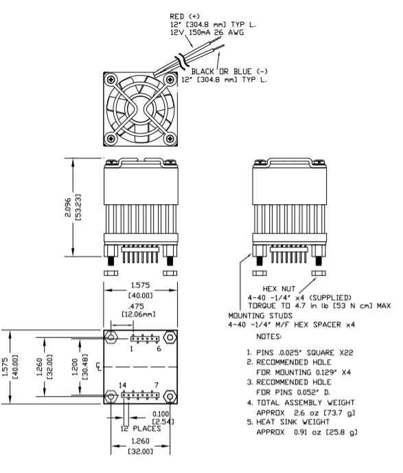
MOUNTING THE AMPLIFIER
The amplifier is supplied with four 4-40 M/F hex spacers at the four corners of the amplifier. Once the amplifier is seated, secure the module with the provided 4-40 nuts and torque to 4.7 in lb [53 N cm] max. See “Dimensional Information” for a detailed drawing. It is recommended that the heat sink be grounded to the system ground. This can easily be done by providing a grounded circuit board pad around any of the holes for the mounting studs.
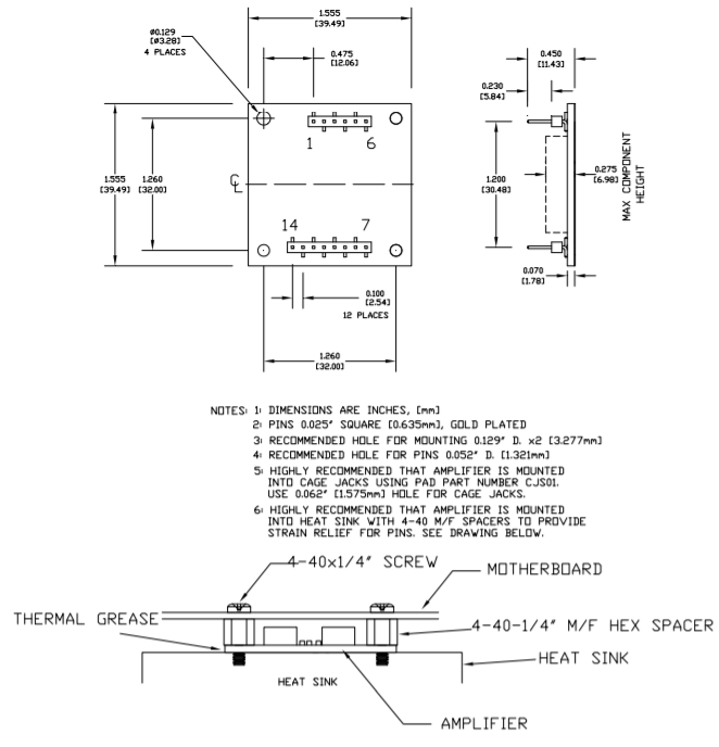
MOUNTING THE PAD138-1 AMPLIFIER
In most applications the amplifier must be attached to a heat sink. Spread a thin and even coat of heat sink grease across the back of the PAD138 and also the heat sink where the amplifier is to be mounted. Push the amplifier into the heat sink grease on the heat sink while slightly twisting the amplifier back and forth a few times to bed the amplifier into the heat sink grease. On the final twist align the mounting holes of the amplifier with the mounting holes in the heat sink and finish the mounting using 4-40 hex male-female spacers. Mount the amplifier to the mother board with 4-40 X 1/4” screws. For all mounting hardware torque to 4.7 in lb [53 N cm] max.
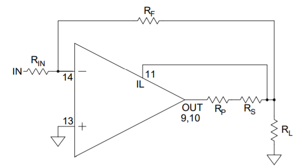
CURRENT LIMIT
The current limiting function is connected as shown in Figure
- It is best to connect Rs directly to OUT to avoid any significant parasitic resistance, Rp, as shown in Figure 1. The sense voltage for current limit is approximately 0.7V. Thus:
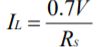
Where IL is the value of the limited current and RS is the value of the current limit sense resistor.
In addition, the sense voltage has a temperature coefficient approximately equal to –2.2mV/℃.
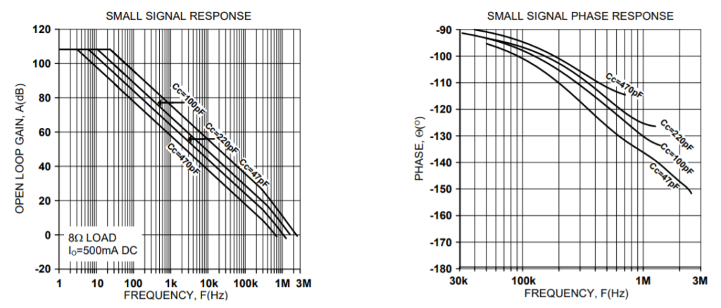
PHASE COMPENSATION
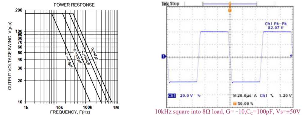
The PAD138 must be phase compensated. The compensation capacitor, CC, is connected between pins 2 and 3. The compensation capacitor must be an NPO type capacitor rated for the full supply voltage (200V). On page 2, under Amplifier Pinout and Connections, you will find a table that gives recommended compensation capacitance value for various circuit gains and the resulting slew rate for each capacitor value. Consult also the small signal response and phase response plots for the selected compensation value in the Typical Performance Graphs section. A compensation capacitor less than 47pF is not recommended.
BOOST OPERATION
The small signal stages of the PAD138 are connected to the ±VCC power supply pins. When the ±VCC voltages are greater than the ±Vs power supply pins the small signal stages of the amplifier are biased so that the output transistors can be driven very close to the ±Vs rails. Close swings to the supply rails increase the efficiency of the amplifier and make better use the supply voltages. This technique is often used to operate the amplifier with only a single high current power supply, thus reducing the system size and cost. Also see the application article AN-22 Single Supply Operation with Power Op Amps for more detailed information and circuits.
TYPICAL PERFORMANCE GRAPHS
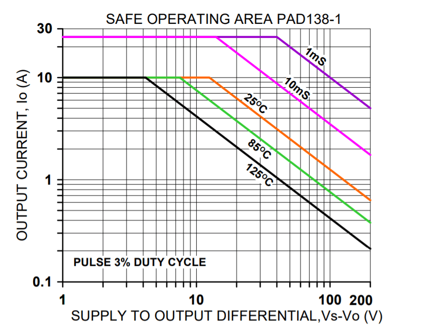
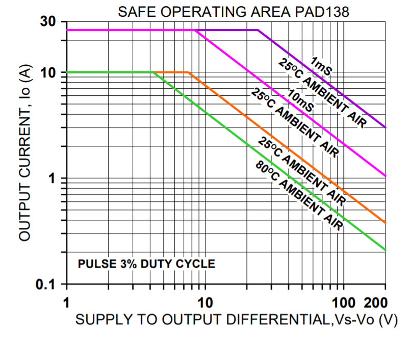
SAFE OPERATING AREA
DIMENSIONAL INFORMATION