Downloads
Datasheet
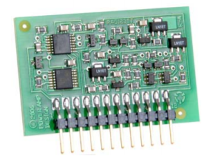
PAD125
Rev E
KEY FEATURES
- LOW COST ACCESSORY
- FLOATING CURRENT SENSE
- MULTIPLE MODE OPERATION
- WIDE SUPPLY RANGE 8V – 250V
- GROUND REFERENCED OUTPUT
- CONVENIENT SIP PIN-OUT
- CONFORMAL COATED
- RoHS COMPLIANT AFTER JUNE 1, 2018
APPLICATIONS
- HIGH POWER AMPLIFIER ADD-ON
- REPLACE LINEAR CURRENT LIMIT
- AMPLIFIER PROTECTION CIRCUIT
DESCRIPTION
The PAD125 current limit accessory module was designed to extend the protection circuitry for high power amplifiers and avoid current limit induced oscillations that often occur in high output current amplifiers. To keep power dissipation in the current sense resistor to a minimum the PAD125 operates with a precision 150mV floating sense input and converts the floating sense inputs to ground referenced 5V logic signals. Traditional current limit circuitry does not guarantee that the amplifier will survive over-current conditions. The PAD125 can operate in several modes. It can latch off the host amplifier when an over-current condition exists immediately or after an externally set time delay set by a simple RC circuit. The circuit can also auto-reset with another RC circuit time delay. In addition the host amplifier can be shut down or reset from system logic inputs. After June 1, 2018 the PAD125 is RoHS compliant and conformal coated.
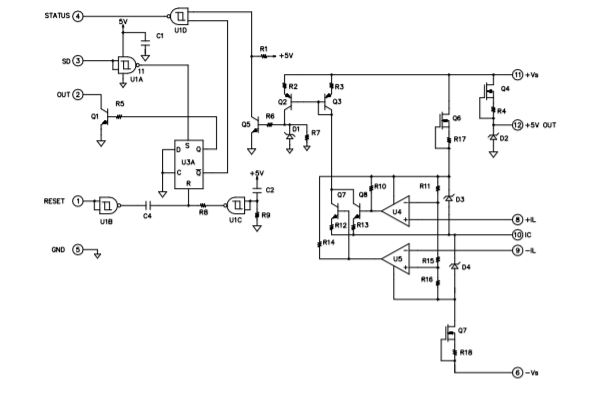
EQUIVALENT CIRCUIT
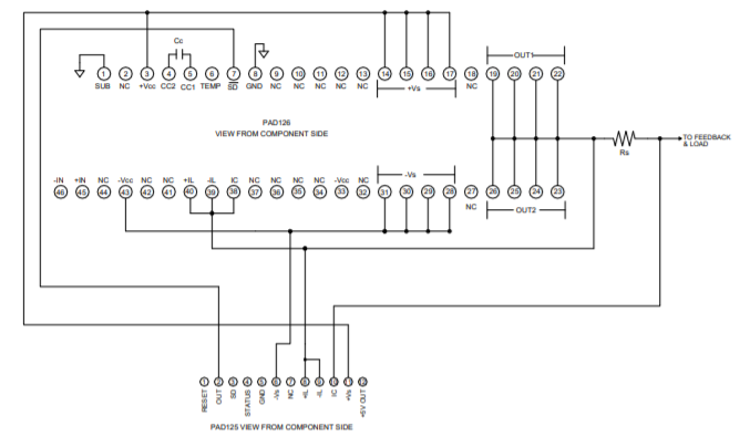
PAD125 TYPICAL CONNECTION TO PAD126
NOTES:
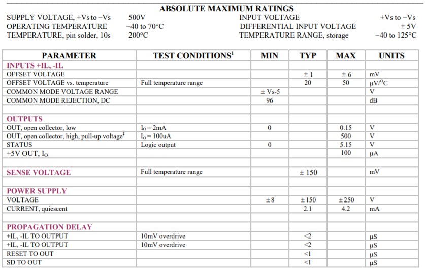
- Unless otherwise noted: TC=25oC
- Power dissipation in the open collector output transistor is limited to 200mW (full temperature range).
COMMON MODE RANGE
The sense voltage inputs of the PAD125 (+IL, -IL, ISC) float with the output of the host amplifier (PAD119, for example) and can swing within 5V of either supply rail
SENSE VOLTAGE
The output (OUT, pin 2) is set to trip (go low) when:
IS-ISC > 150mV
or
ISC-IS > 150mV
Where IS represents +IL and -IL tied together for normal operation. +IL and -IL can be separated for fold-over current limiting. For fold-over current limit operation OUT is set to trip when:
(+IL)-ISC> 150mV
or
ISC-(-IL) > 150mV
This 150mV reference is generated internally and cannot be changed by the user. In all cases the circuit is tripped when:
Io > ±150mV/Rs
where Io is the host amplifier output current and Rs is the current limit sense resistor value.
OUTPUT
The output (OUT, pin 2) is an open collector circuit and is intended to be tied to the host amplifier SD input. The SD input of the host amplifier has an internal pull-up circuit so if OUT is used without the host amplifier an external 10k pull-up resistor will be required.
STATUS OUTPUT
STATUS, pin 4, is the output that alerts external circuitry that the current set point has been exceeded and goes high (5V logic) when this occurs. In various modes of operation STATUS is connected to the shutdown input (SD) and/or RESET. See “Applications Circuits” for illustrations on how to use the several modes of operation.
SD AND RESET INPUTS
The SD (shutdown) and RESET inputs can be operated from system logic signals as required. These are 5V logic inputs. If not used these inputs are required to be tied to ground or pulled down by 10kΩ. If these inputs are operated from an open collector circuit an external pull up resistor is required. Do not confuse the SD input of the PAD125 with the SD input of the host amplifier.
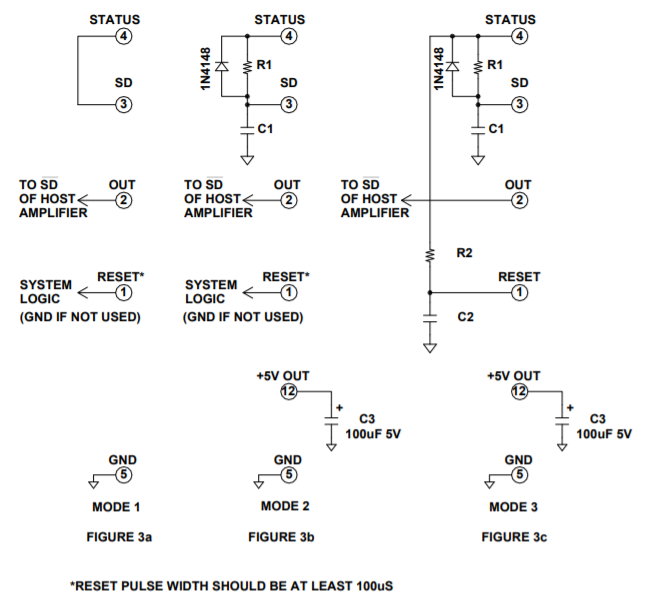
OPERATING MODES
It is possible to operate the PAD125 in several modes without the need for any external logic circuits by using a few external passive components. For each of the operating modes see Figure 3 in “Application Circuits”.
In Mode 1 (Figure 3a) the STATUS output is tied directly to SD. When the output current of the host amplifier exceeds the trip point, OUT immediately goes low and latches off the output stage of the host amplifier. To restart the host amplifier a “high” on the RESET pin is required.
In Mode 2 (Figure 3b) the STATUS output is tied to the SD input through a RC circuit (R1, C1). The RC circuit provides a time delay. This is useful when, for example, it is known that the host amplifier output current will exceed the set point current for a short time and still not exceed the SOA of the amplifier. This might occur when starting a motor, for example. The time delay can be calculated by:
T=RC
Where T is the time delay, R is the resistance in ohms and C is the capacitance in farads. The minimum resistor value is 100kΩ and the maximum C value is 2.2nF.
In Mode 3 (Figure 3c) an auto-reset can be applied by adding R2, C2 to the RESET input. This time delay must be greater than R1, C1 but operates in the same way and is calculated in the same way. Mode 3 can be used with Mode 1 if desired. In this mode if the over-current condition still exits after the reset time delay the PAD125 will keep the host amplifier shut down indefinitely. The circuit can be restarted by cycling the power or over driving the reset input with a momentary external 5V pulse.
Note that any unused input pins must be grounded (pins
1 or 3).
EVALUATION KITS
Connections for the PAD125 are incorporated into the printed circuit boards included with evaluation kits for compatible amplifier models. Either standard or fold over current limit can be implemented. Bread-boarding pads are provided to connect the PAD125 in any of the operating modes discussed above. PAD Power™ is a free Excel based spreadsheet available on the Power Amp Design website that will assist in calculating values needed to implement the fold-over current limit as well as analyzing many other design issues when using Power Amp Design products.
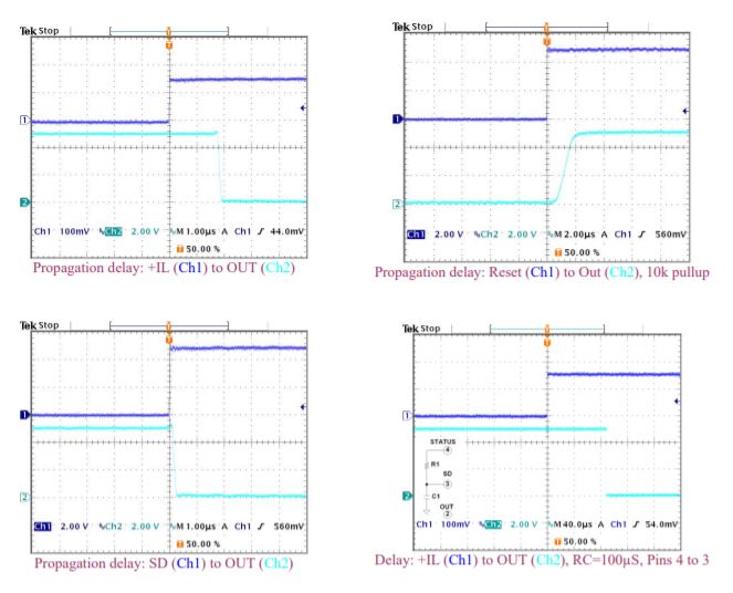
TYPICAL PERFORMANCE GRAPHS
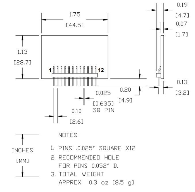
DIMENSIONAL INFORMATION
APPLICATION CIRCUITS
OPERATING MODES