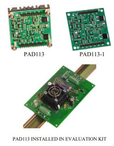
PAD113
Rev I
KEY FEATURES
- LOW COST
- HIGH VOLTAGE – 500 VOLTS
- HIGH OUTPUT CURRENT –1.5A
- 29 WATT DISSIPATION CAPABILITY
- 97 WATT OUTPUT CAPABILITY
- INTEGRATED HEAT SINK AND FAN
APPLICATIONS
- PIEZO TRANSDUCER DRIVE
- HIGH VOLTAGE INSTRUMENTATION
- SEMICONDUCTOR TESTING
DESCRIPTION
The PAD113 high voltage operational amplifier is constructed with surface mount components to provide a cost effective solution for many industrial applications. With a footprint only 3.8 in2 the PAD113 offers outstanding performance that rivals much more expensive hybrid component amplifiers or rack-mount amplifiers. User selectable external compensation tailors the amplifier’s response to the application requirements. Four-wire programmable current limit is built-in. The PAD113 also features a substrate temperature reporting output and overtemp shutdown. The amplifier circuitry is built on a thermally conductive but electrically insulating substrate mounted to an integral heat sink and fan assembly. No BeO is used in the PAD113. The resulting module is a small, high performance turn-key solution for many industrial applications. For custom applications the PAD113-1 is also available without the heat sink and fan.
A NEW CONCEPT
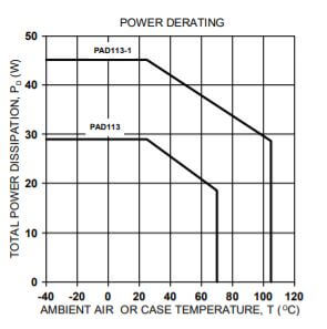
A critical task in any power amplifier application is cooling the amplifier. Until now component amplifier manufacturers often treated this task as an after-thought, left for the user to figure out. At Power Amp Design the best heat sink and fan is chosen at the start and becomes an integral part of the overall amplifier design. The result is the most compact and volumetric efficient design combination at the lowest cost. In addition, this integrated solution concept offers an achievable real-world power dissipation rating, not the ideal rating usually cited when the amplifier case is somehow kept at 25o C. The user no longer needs to specify, procure or assemble separate components.
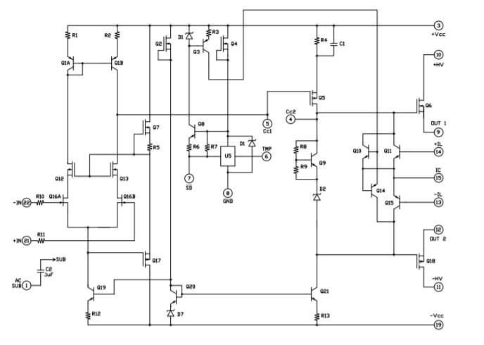
CIRCUIT & CONNECTIONS
EQUIVALENT CIRCUIT
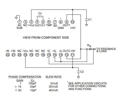
PINOUT & CONNECTIONS
ABSOLUTE MAXIMUM RATINGS SPECIFICATIONS
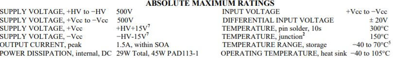
Notes:
- Unless otherwise noted: TC=25OC, compensation Cc=220pF, DC input specifications are value given, power supply voltage is typical rating.
- Derate internal power dissipation to achieve high MTBF.
- Doubles for every 10OC of case temperature increase.
- +HV and −HV denote the positive and negative supply voltages to the output stage. +Vcc and −Vcc denote the positive and negative supply voltages to the input stages.
- Limited by fan characteristics. During operation, even though the heat sink may be at 85OC or more the fan will be at a lower temperature.
- Rating applies if the output current alternates between both output transistors at a rate faster than 60Hz.
- Power supply voltages +Vcc and −Vcc must not be less than +HV and −HV respectively. Total voltage +Vcc to −Vcc 500V maximum.
- L10 refers to the time it takes for 10% of a population of fans to fail. Lower ambient temperature increases fan life.
- Specifications for the PAD113-1 are the same as for the PAD113 except as shown in this column.
OPERATING CONSIDERATIONS
SAFETY FIRST
The operating voltages of the PAD113 are potentially deadly. When developing an application circuit it is wise to begin with power supply voltages as low as possible while checking for circuit functionality. Increase supply voltages slowly as confidence in the application circuit increases. Always use a “hands off” method whereby test equipment probes are attached only when power is off. See application note AN-16 for PCB layout guidelines.
EXTERNAL CIRCUIT COMPONENTS
The output of the PAD113 can swing up to +/- 240V and this may stress or destroy external components that are often not seriously considered when developing circuits with small signal op amps. High voltage rated resistors may be purchased for the feedback circuit or, alternately, several ordinary resistors may be placed in series to obtain the proper voltage rating. The compensation capacitor CC is a NPO type and is rated for 500V. See AN-16 for PCB layout guidelines.
COOLING FAN
The PAD113 relies on its fan for proper cooling of the amplifier. Make sure that air flow to the fan and away from the heat sink remains unobstructed. To eliminate electrical noise created by the cooling fan we recommend a 47µF capacitor placed directly at the point where the fan wires connect to the PCB. See application note AN-24 for further details.
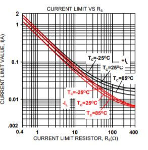
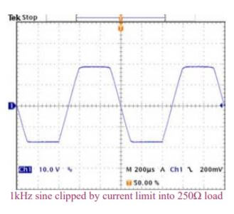
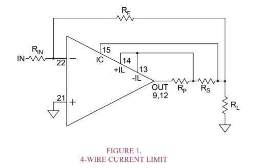
CURRENT LIMIT
The current limiting function of the PAD113 is a versatile circuit that can be used to implement a four-wire current limit configuration or, in combination with some external components can be configured to implement a fold-over current limit circuit. The four-wire current limit configuration insures that parasitic resistance in the output line, Rp, does not affect the programmed current limit setting. See Figure 1. The sense voltage for current limit is 0.63V. Thus approximately

Where IL is the value of the limited current and RS is the value of the current limit sense resistor from 0.4Ω-40Ω. See graph for Current Limit Value vs RS.
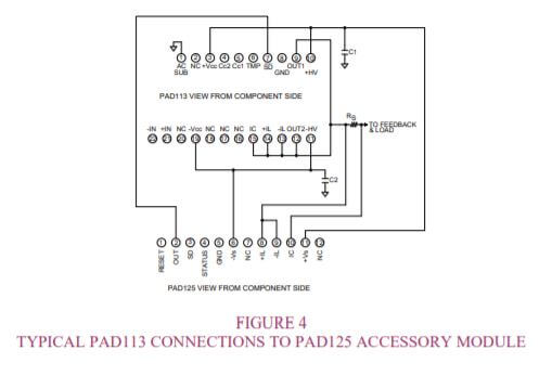
In addition, the sense voltage has a temperature coefficient approximately equal to –2.2mV/o C. The fold-over function reduces the available current as the voltage across the output transistors increases to help insure that the SOA of the output transistors is not exceeded. Refer to Application Circuits for details on how to connect the current limit circuitry to implement either a four-wire current limit or current limit with a fold-over function. The PAD113 is also compatible with the precision PAD125 Current Limit Accessory Module. See Figure 4 and the datasheet for the PAD125 for further details.
MOUNTING THE AMPLIFIER
The amplifier is supplied with four 4-40 M/F hex spacers at the four corners of the amplifier. Once the amplifier is seated, secure the module with the provided 4-40 nuts and torque to
4.7 in lb [53 N cm] max. See “Dimensional Information” for a detailed drawing. It is recommended that the heat sink be grounded to the system ground. This can easily be done by providing a grounded circuit board pad around any of the holes for the mounting studs.
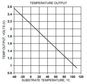
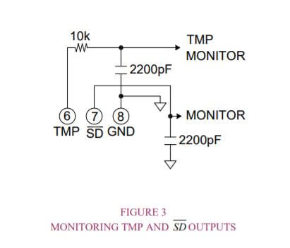
TEMPERATURE REPORTING
An analog output voltage is provided (pin 6, TMP) relative to ground and proportional to the temperature in degrees C. The slope is approximately -10.82mV/o C. The output voltage follows the equation:
T = (2.127 ─ V) (92.42)
Where V is the TMP output voltage and T is the substrate temperature in degrees C.
This high impedance output circuit is susceptible to capacitive loading and pickup from the output of the amplifier. When monitoring TMP filter the voltage as shown in Figure 3. See Applications Circuits.
THERMAL SHUTDOWN
The temperature monitoring circuit automatically turns off the amplifier when the substrate temperature reaches 110o C. When the substrate cools down 10o C the amplifier is enabled once again. The thermal shutdown feature is activated either by amplifier overloads or a failure of the fan circuit.
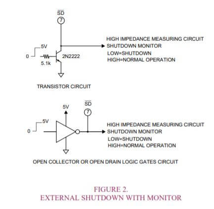
EXTERNAL SHUTDOWN
When pin 7 ( SD ) is taken low (ground) the amplifier is turned “off” and remains “off” as long as pin 7 is low. When pin 7 is monitored with a high impedance circuit it also functions as a flag, reporting when the amplifier is shut down. A “high” (+5V) on pin 7 indicates the temperature is in the normal range. A “low” (ground) indicates a shutdown condition. See Application Circuits for details on how to implement an external shutdown circuit and how to monitor the shutdown status when temperature is in the normal range. A “low” (ground) indicates a shutdown condition. See Application Circuits for details on how to implement an external shutdown circuit and how to monitor the shutdown status.
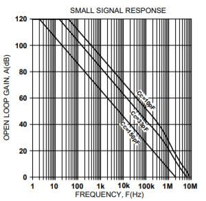
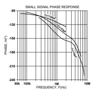
PHASE COMPENSATION
The PAD113 must be phase compensated. The compensation capacitor, CC, is connected between pins 4 and 5. The compensation capacitor must be an NPO type capacitor rated for the full supply voltage (500V). On page 2, under Amplifier Pinout and Connections, you will find a table that gives recommended compensation capacitance value for various circuit gains and the resulting slew rate for each capacitor value. Consult also the small signal response and phase response plots for the selected compensation value in the Typical Performance Graphs section. A compensation capacitor less than 10pF is not recommended.
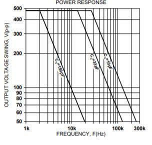
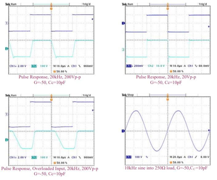
TYPICAL PERFORMANCE GRAPHS
PERFORMANCE GRAPHS CONTINUED
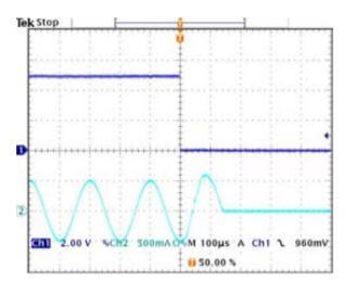
SHUTDOWN RESPONSE, POSITIVE OUTPUT TO ZERO TRANSITION
The oscilloscope display at the right shows a view of a 5kHz, 1A p-p amplifier output signal being interrupted near the positive peak by a shutdown signal on Ch1. The Ch2 display shows the output current going to zero about 50µS after the shutdown signal goes low.
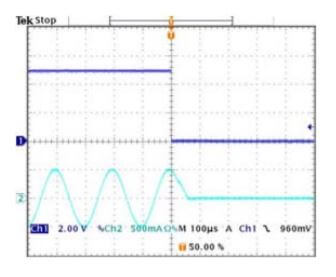
SHUTDOWN RESPONSE, NEGATIVE OUTPUT TO ZERO TRANSITION
The oscilloscope display at the left shows a view of a 5kHz, 1A p-p amplifier output signal being interrupted near the negative peak by a shutdown signal on Ch1. The Ch2 display shows the output current going to zero about 150µS after the shutdown signal goes low.
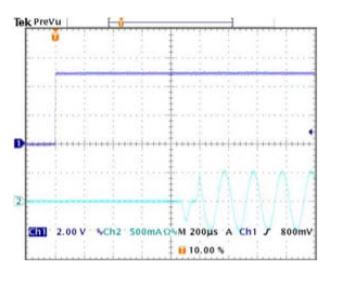
SHUTDOWN RECOVERY
The oscilloscope display at the left shows a view of a 5kHz, 1A p-p amplifier output signal on Ch2 resuming normal operation after a shutdown signal on Ch1 go high (not shutdown). The output signal resumes normal operation after a delay of about 1mS.
SAFE OPERATING AREA
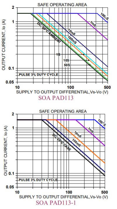
SAFE OPERATING AREA
The safe operating area (SOA) of a power amplifier is its single most important specification. The SOA graph presented above serves as a first approximation to help you decide if the PAD113 will meet the demands of your application. But a more accurate determination can be reached by making use of the PAD Power™ spreadsheet which can be found in the Power Amp Design website under Design Spreadsheet tab. While the graph above adequately shows DC SOA and some pulse information it does not take into account ambient temperatures higher than 30OC, AC sine, phase or non-symmetric conditions that often appear in real-world applications. The PAD Power™ spreadsheet takes all of these effects into account.
DIMENSIONAL INFORMATION
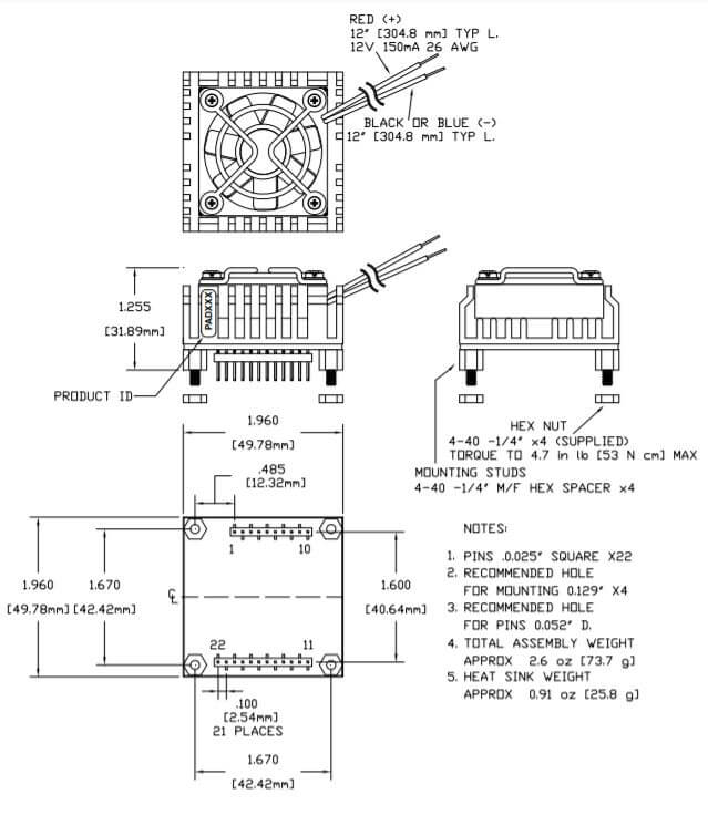
DIMENSIONAL INFORMATION CONTINUED

APPLICATION CIRCUITS
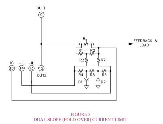
With the three current limit function pins (pins 13-15) dual slope current limiting can be implemented that more closely approximates the SOA curve of the amplifier than can be achieved with standard current limiting techniques. Values for resistors R1-R7 and RS can be calculated using the PAD Power™ Excel spreadsheet that can be downloaded from the Power Amp Design web site under the Design Spreadsheet tab