Downloads
Datasheet
PAD111
Rev C
KEY FEATURES
- LOW COST
- HIGH VOLTAGE – 100 VOLTS
- HIGH CURRENT – 15 AMPS
- 170 WATT DISSIPATION CAPABILITY
- 500kHz POWER BANDWIDTH
- 130 V/µS SLEW RATE
- PROGRAMMABLE CURRENT LIMIT
- RoHS COMPLIANT
APPLICATIONS
- INKJET PRINTER HEAD DRIVE
- PIEZO TRANSDUCER DRIVE
- INDUSTRIAL INSTRUMENTATION
- RELECTOMETERS
- ULTRA-SOUND TRANSDUCER DRIVE
DESCRIPTION
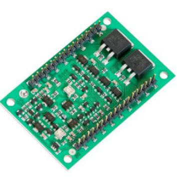
The PAD111 is a high voltage operational amplifier constructed with surface mount components to provide a cost effective solution for many industrial applications With a footprint only 3.3in2 the PAD111 offers outstanding performance that rivals more expensive hybrid component amplifiers. User selectable external compensation tailors the amplifier’s response to the application requirements. Four-wire current limit is built-in. The amplifier circuitry is built on a thermally conductive but electrically insulating substrate. No BeO is used in the PAD111. The resulting module is a small, high performance solution for many industrial applications.
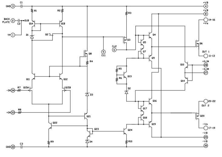
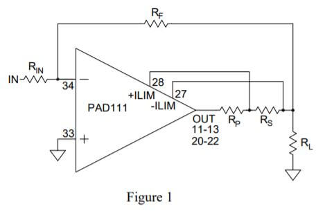
CIRCUIT & CONNECTIONS
EQUIVALENT CIRCUIT
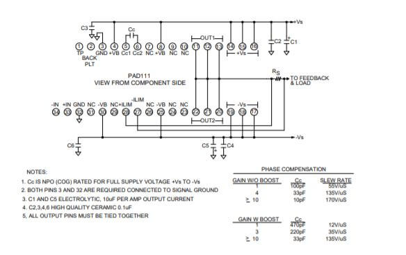
PINOUT & CONNECTIONS
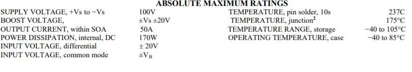
ABSOLUTE MAXIMUM RATINGS SPECIFICATIONS
NOTES:
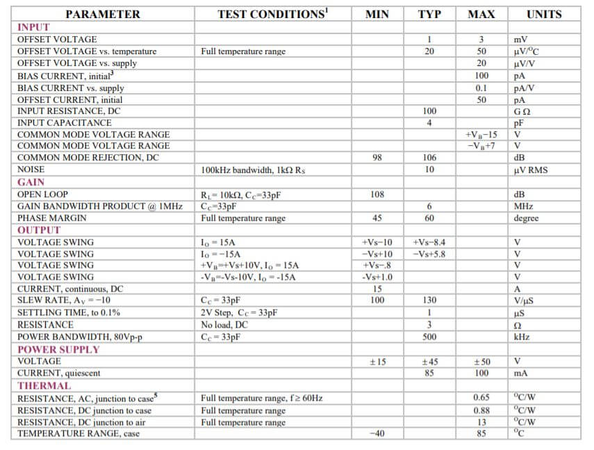
- Unless otherwise noted: TC = 25OC, compensation Cc = 100pF, DC input specifications are value given, power supply voltage is typical rating.
- Derate internal power dissipation to achieve high MTBF.
- Doubles for every 10OC of case temperature increase.
- +Vs and −Vs denote the positive and negative supply voltages to the output stage. +VB and −VB denote the positive and negative supply voltages to the input stages.
- Rating applies if the output current alternates between both output transistors at a rate faster than 60Hz.
- Power supply voltages +VB and −VB must not be less than +Vs and −Vs respectively. Total voltage +VB to −VB 140V maximum.
- The PAD111 is constructed with MOSFET transistors and ESD handling procedures must be observed.
OPERATING CONSIDERATIONS
SAFETY FIRST
The operating voltages of the PAD111 are potentially deadly. When developing an application circuit it is wise to begin with power supply voltages as low as possible while checking for circuit functionality. Increase supply voltages slowly as confidence in the application circuit increases. Always use a “hands off” method whereby test equipment probes are attached only when power is off.
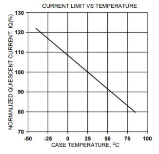
CURRENT LIMIT
The current limiting function of the PAD111 is a versatile circuit that can be used to implement a four-wire current limit configuration. The four-wire current limit configuration insures that parasitic resistance in the output line, Rp, does not affect the programmed current limit setting. See Figure 1 below. The sense voltage for current limit is 0.65V. Thus:

Where IL is the value of the limited current and RS is the value of the current limit sense resistor.
In addition, the sense voltage has a temperature coefficient approximately equal to –2.2mV/o C.
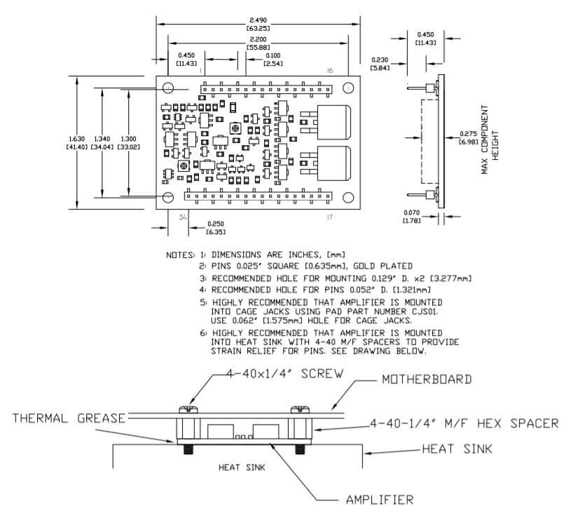
MOUNTING THE AMPLIFIER
In most applications the amplifier must be attached to a heat sink. Spread a thin and even coat of heat sink grease across the back of the PAD111 and also the heat sink where the amplifier is to be mounted. Push the amplifier into the heat sink grease on the heat sink while slightly twisting the amplifier back and forth a few times to bed the amplifier into the heat sink grease. On the final twist align the mounting holes of the amplifier with the mounting holes in the heat sink and finish the
mounting using 4-40 hex male-female spacers. Mount the amplifier to the mother board with 4-40 X 1/4” screws.
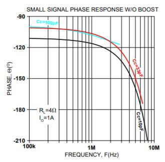
PHASE COMPENSATION
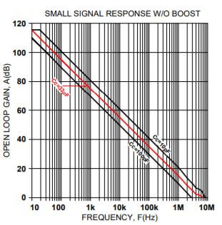
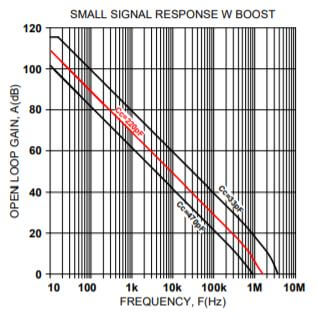
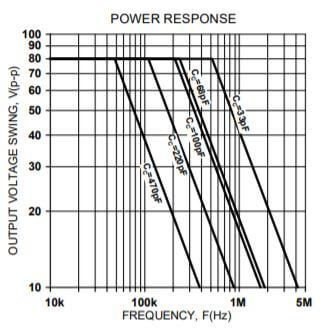
The PAD111 must be phase compensated. The compensation capacitor, CC, is connected between pins 5 and 6. The compensation capacitor must be an NPO type capacitor rated for the full supply voltage (100V). On page 2, under Amplifier Pinout and Connections, you will find a table that gives recommended compensation capacitance value for various circuit gains and the resulting slew rate for each capacitor value. Consult also the small signal response and phase response plots for the selected compensation value in the Typical Performance Graphs section Do not use a compensation capacitor less than 10pF.
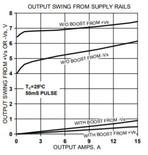
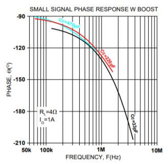
BOOST OPERATION
The small signal stages of the PAD111 are connected to the ±VB power supply pins. When the ±VB voltages are greater than the ±Vs power supply pins the small signal stages of the amplifier are biased so that the output transistors can be driven very close to the ±Vs rails. Close swings to the supply rails increase the efficiency of the amplifier and make better use the supply voltages. This technique is often used to operate the amplifier with only a single high current power supply, thus reducing the system size and cost. Also see the application article AN-22 Single Supply Operation with Power Op Amps for more detailed information and circuits.
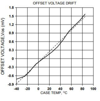
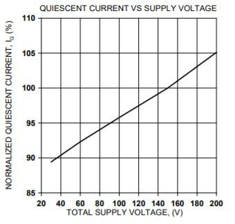
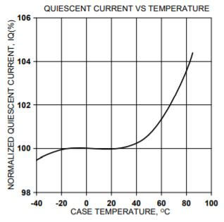
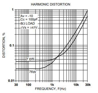
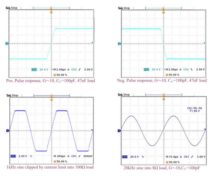
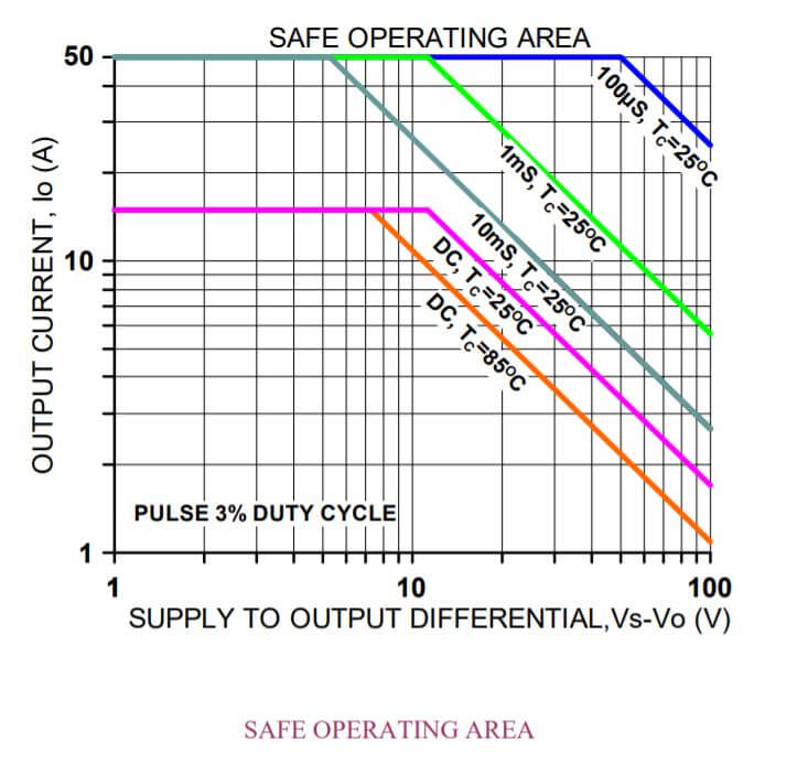
TYPICAL PERFORMANCE GRAPHS
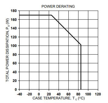
SAFE OPERATING AREA
DIMENSIONAL INFORMATION