Downloads
Datasheet
EVAL541
Rev A
INTRODUCTION
The EVAL541 evaluation kit provides a convenient method to become familiar with the operation of amplifier model PAD541 before your application circuit is committed to production. Some assembly is required since user selections are needed depending on the application. For example, a current limit resistor value needs to be selected by the user. Also, there are two PCB mounting options available.
Critical connections for power supply bypassing and compensation are pre-wired. Connections are also provided for diode clamps on each power supply and the output for those applications in which significant inductive kickback may be found. Terminal strips are also provided for input and output signals and power.
ASSEMBLY STEPS
Please note that the #1 cause of problems for evaluation kit users is not reading and following the directions (all of them). The #2 cause of problems is poor solder joints (cold or bridging). Don’t become a statistic. each step.
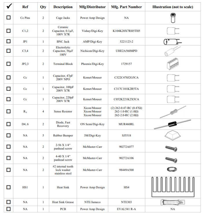
Refer to the Illustrated Parts List for the components mentioned in the assembly steps. Note that some heavy PCB copper planes and some heavy component leads are soldered in this kit. This may require a larger soldering iron tip and/or higher soldering iron temperatures than might normally be used. These steps are marked with an asterisk (*).
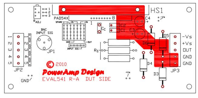
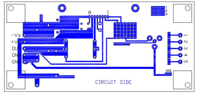
1. Notice that the printed circuit board (PCB) is labeled on one side as the “DUT SIDE” and the other side as “CIRCUIT SIDE”.
2.* Four current limiting sense resistors, RS, are provided; two 0.47 Ω, one 1.0 Ω and one 2.0 Ω. Likewise, there are four locations on the PCB for these resistors. The PCB ties all four of the locations in parallel. The resistors can be used individually at any location or several can be used to fine tune the final value desired. See the datasheet for the amplifier to determine the best value for your application. Solder the resistor(s) from the “CIRCUIT SIDE” of the PCB.
3. D3 and D5 are transient voltage suppressor diodes and are not supplied since the type (breakdown voltage) varies with the application. They are not necessary for every application. They are most commonly used in application circuits where kickback from the load may force the supply voltage above the limits of the amplifier.
4. The evaluation kit PCB can be mounted in several ways.
Option 1- Chassis mount. Use #6 standoffs and screws (not supplied) attached to the PCB at the four corners of the PCB.
Option 2- Bench-top mount. Use the rubber bumpers supplied. These are “stick-on” components. Remove the release paper from each bumper and apply the bumper to the square outlines on the “CIRCUIT SIDE” of the PCB.
5. Slightly loosen the 4-40 screws that hold the heat sink to the PCB.
6. Spread a thin and even coat of heat sink grease across the back of the PAD541 and also the heat sink where the amplifier is to be mounted. Insert the PAD541 pins into the holes of the PCB at the mounting location next to HS1. Push the amplifier into the heat sink grease on the heat sink while slightly moving the amplifier up and down a few times to bed the amplifier into the heat sink grease. On the final movement align the mounting holes of the amplifier with the mounting holes in the heat sink and finish the mounting using 2-56 screws and #2 stainless steel internal tooth lock washers. The lock washers help to electrically connect the substrate to the heat sink (that is grounded). Torque the screws to 2.2 in-pound (0.248 N meter) maximum. Do not rely on the screw pressure to squeeze out any excess heat sink grease as this will likely only bend the substrate at the corners.
7. Tighten the 4-40 heat sink mounting screws and solder the leads of the amplifier from the “CIRCUIT SIDE” of the PCB. Solder the pins of the PAD541.
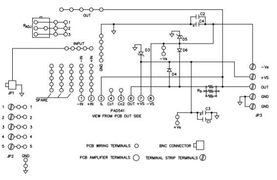
8. Use the bread-boarding area to add the external components necessary to program the amplifier gain and other circuit requirements to evaluate your application circuit. You can use the evaluation kit schematic and PCB views to map out your circuit
ASSEMBLY STEPS CONTINUED
9. Remember that the amplifier must be compensated to operate correctly. See the amplifier datasheet on Page 4, under PHASE COMPENSATION. The selected phase compensation capacitor will be installed at “CC” on the evaluation kit PCB. A 220pF capacitor has already been installed in your kit. Another value may better suit your application. Remove and replace the capacitor as necessary for your application. 47pF and 100pF capacitors are also included with the kit. CC must be rated for at least 100V. A temperature stable type capacitor is required— an X7R ceramic, for example, or an NPO typ
10. The evaluation kit assembly is complete. Be sure you have read and followed all the assembly steps. Inspect the circuit board for solder shorts or poor solder joints. An illuminated magnifier is helpful.
11. Before applying power to your circuit set the power supply for ±20V and set the power supply current limit to approximately 100mA. Use little or no load at first. Apply an input signal and check the output with an oscilloscope to verify proper functionality. This step can prevent damaging the amplifier or the circuit board should there be some mistake in assembly.
ILLUSTRATED PARTS LIST
Note that the amplifier is purchased separately.
CIRCUIT & CONNECTIONS
CIRCUIT DIAGRAM
PCB VIEWS
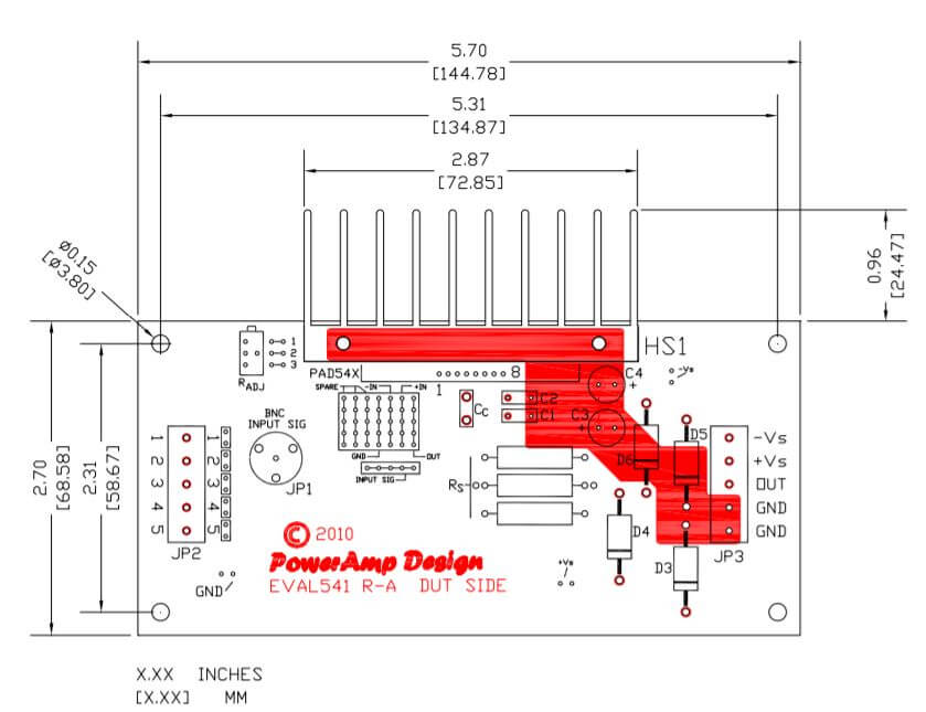
TOP VIEW
BOTTOM VIEW
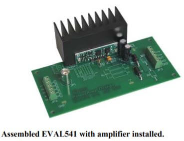
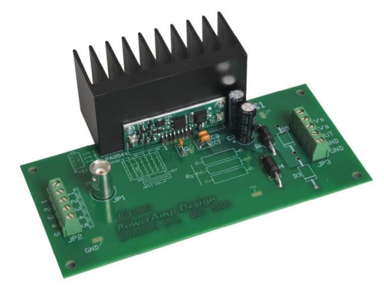
ASSEMBLED KIT
ASSEMBLED EVAL541 WITH AMPLIFIER MOUNTED
DIMENSIONAL INFORMATION
BOARD OUTLINE DIMENSIONS