Downloads
Datasheet
EVAL138
Rev C
INTRODUCTION
The EVAL138 evaluation kit provides a convenient method to become familiar with the operation of amplifier models PAD138, PAD139 or PAD141 before your application circuit is committed to production. Some assembly is required since user selections are needed depending on the application. For example, a current limit resistor will be selected. There are also several PCB mounting options available.
Critical connections for power supply bypassing and compensation are pre-wired. Connections are also provided for diode clamps on each power supply and the output for those applications in which significant inductive kickback may be found. Terminal strips are also provided for input and output signals and power.
ASSEMBLY STEPS
Please note that the #1 cause of problems for evaluation kit users is not reading and following the directions (all of them). The #2 cause of problems is poor solder joints (cold or bridging). Don’t become a statistic. each step.
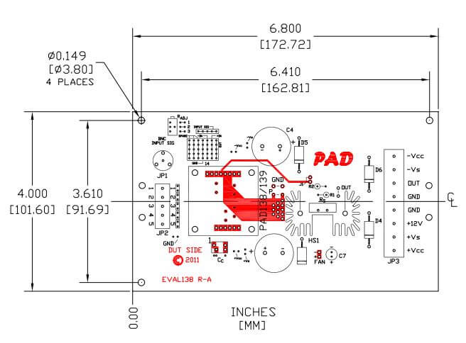
1. Notice that the printed circuit board (PCB) is labeled on one side as the “DUT SIDE” and the other side as “CIRCUIT” side.
2. D3 and D5 are transient voltage suppressor diodes and are not supplied since the type (breakdown voltage) varies with the application. They are not necessary for every application. They are most commonly used in application circuits where kickback from the load may force the supply voltage above the limits of the amplifier.
3. The evaluation kit PCB can be mounted in several ways.
Option 1- Chassis mount. Use #6 standoffs and screws (not supplied) attached to the PCB at the four corners of the PCB.
Option 2- Bench-top mount. Use the rubber bumpers supplied. These are “stick-on” components. Remove the release paper from each bumper and apply the bumper to the square outlines on the “CIRCUIT SIDE” of the PCB.
Option 3- DIN rail mount. The PCB can be mounted to a 35mm DIN rail. For mounting the PCB to a DIN rail press the adaptors into the PCB in the holes at the edges of the PCB at locations 1 and 2 from the “CIRCUIT SIDE” of the PCB. Make sure that the plastic tines have fully spread out on the “DUT SIDE” of the PCB.
4. Several current limiting resistors are provided: one 100mΩ, one 200mΩ and one 500mΩ. Follow the amplifier model’s datasheet to determine which resistor value to use for your application. The current limit circuit is not a precision
circuit, but the approximate current limit value can be determined by:

Where IL is the desired current limit value and Rs is the current limit sense resistor value
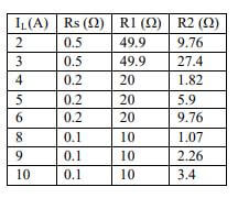
Using the supplied current limit sense resistors (Rs) the current limit values obtainable are:

Other values of current limit are possible using the Rs values in this kit by utilizing the R1, R2 divider (and removing the jumper J1). A suitable method for determining the values of R1 and R2 is to first select a sense resistor such that IL X Rs > 0.7V. For example, if you wanted a current limit value of 2A you would select the 500mΩ resistor. Next, assign R1 a value of 100Rs (this assignment keeps the power dissipation of R1 within the ¼ watt rating of common resistors) and solve for R2 in the following equation:
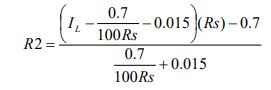
Where IL is the desired current limit value and Rs is the current limit sense resistor value.
ASSEMBLY STEPS CONTINUED
For example, when a current limit of 2A is desired Rs is 500mΩ, R1 is 50Ω and R2 is 9.83Ω. Standard 1% values of 49.9Ω and 9.76Ω are adequate substitutions.
In the table below standard 1% values for R2 and R1 are listed for a variety of common current limit values.
Smear a small amount of heat sink grease on the back of the selected resistor (RS) and then attach the resistor to heat sink HS1 at RS with a 4-40 X ½” screw and nut. The plastic nut driver supplied with this kit will help here. Tighten the 4-40 resistor mounting hardware. Solder the resistor from the “CIRCUIT SIDE” of the PCB making sure that the holes are completely filled with solder.
5. Remove the 4 hex nuts from the mounting spacers of the amplifier.
6. Align the 4 studs of the mounting spacers with the mounting holes in the PCB. Be sure that the amplifier’s pin 1 aligns with pin 1 on the PCB. Slowly lower the amplifier into the PCB, making sure that the pins of the amplifier and the cage jacks mate. Push the amplifier into the PCB until the mounting spacers meet the PCB.
7. Fasten the amplifier to the PCB with the 4 hex nuts previously removed. Do not over-tighten the nuts as this may strip the mounting studs. The provided plastic nut starter can assist you here.
8. If necessary, strip 1/8” of insulation from the wires connected to the fan. Twist and tin the wire ends. Insert the red wire into the cage jack labeled “+” and the black or blue wire into the jack marked “─” at the location marked “FAN”. Do not solder the fan wires into the PCB.
9. Use the bread-boarding area to add the external components necessary to program the amplifier gain and other circuit requirements to evaluate your application circuit. You can use the evaluation kit schematic and PCB views to map out your circuit.
10. Remember that the amplifier must be compensated to operate correctly. See the amplifier datasheet on Page 4, under PHASE COMPENSATION. The selected phase compensation capacitor will be installed at “CC” on the evaluation kit PCB. A 470pF capacitor has already been installed in your kit. Another
value may better suit your application. Remove and replace the capacitor as necessary for your application. 33pF and 100pF capacitors are also included with the kit. CC must be rated for at least 200V. A temperature stable type capacitor is required—an X7R ceramic, for example, or an NPO type.
11. The evaluation kit assembly is complete. Be sure you have read and followed all the assembly steps. Do not forget to remove J1 if you are using R1, R2 to modify the current limit set point. Inspect the circuit board for solder shorts or poor solder joints. An illuminated magnifier is helpful.
12. Before applying power to your circuit set the power supply for ±20V and set the power supply current limit to approximately 100mA. Use little or no load at first. Apply an input signal and check the output with an oscilloscope to verify proper functionality. This step can prevent damaging the amplifier or the circuit board should there be some mistake in assembly.
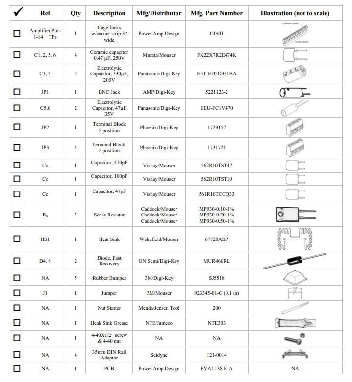
ILLUSTRATED PARTS LIST
Note that the amplifier is purchased separately.
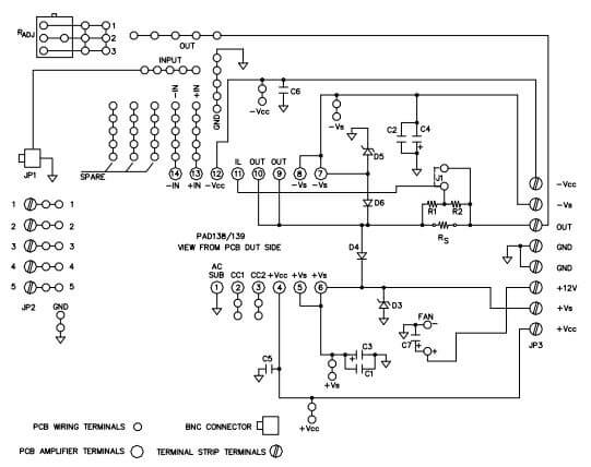
CIRCUIT & CONNECTIONS
CIRCUIT DIAGRAM
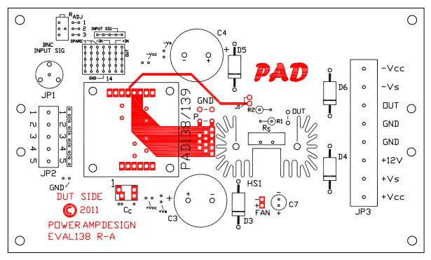
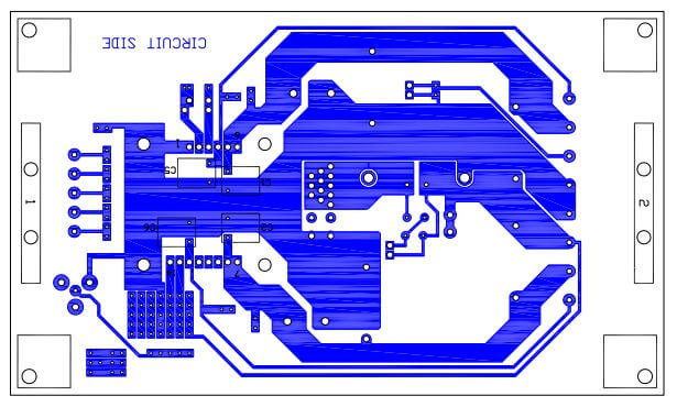
PCB VIEWS
TOP VIEW
BOTTOM VIEW
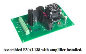
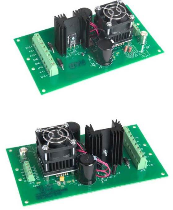
ASSEMBLED KIT
ASSEMBLED EVAL138 WITH AMPLIFIER MOUNTED
DIMENSIONAL INFORMATION
BOARD OUTLINE DIMENSIONS