Downloads
Datasheet
EVAL117
Rev M
INTRODUCTION
The EVAL117 evaluation kit provides a convenient method to become familiar with the operation of the PAD117A operational amplifier before your application circuit is committed to production. Some assembly is required since user selections are needed depending on the application. For example, a current limit resistor value needs to be selected by the user. Also, there are several PCB mounting options available.
Critical connections for power supply bypassing and compensation are pre-wired. Fold-over current limit components are not provided since each application will have different requirements. Connections are also provided for diode clamps on each power supply and the output for those applications in which significant inductive kickback may be found. Terminal strips are also provided for input and output signals and power.
ASSEMBLY STEPS
Please note that the #1 cause of problems for evaluation kit users is not reading and following the directions (all of them). The #2 cause of problems is poor solder joints (cold or bridging). Don’t become a statistic. each step.
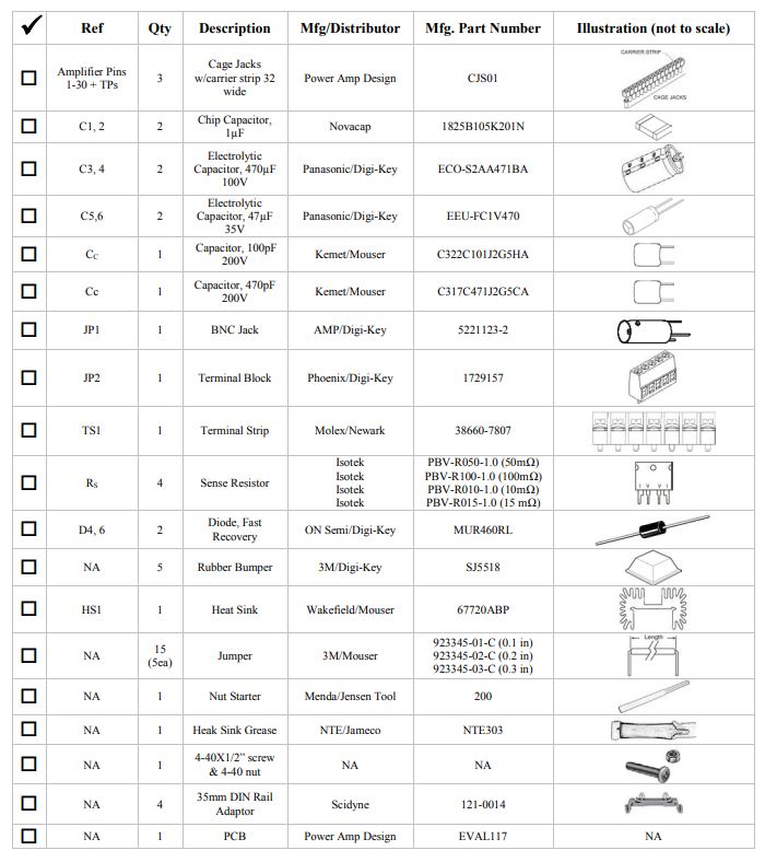
Refer to the Illustrated Parts List for the components mentioned in the assembly steps. Note that some heavy PCB copper planes and some heavy component leads are soldered in this kit. This may require a larger soldering iron tip and/or higher soldering iron temperatures than might normally be used. These steps are marked with an asterisk (*). Note that the pcb may be marked as “PAD117” and “PAD121”. The models PAD117A and PAD125 replace these older models respectively that may be referred to on the pcb.
1. Notice that the printed circuit board (PCB) is labeled on one side as the “DUT SIDE” and the other side as “CIRCUIT” side.
2. As shown in the illustrated parts list, one or more of PAD’s accessory cage jack strip CJS01 was used in the assembly of this kit. It may be advisable to use the cage jack strips in your production circuit board as well. The CJS01 cage jack sockets provide a convenient and inexpensive socket. Soldering and/or de-soldering the amplifier from the circuit board can be extremely difficult due to the high thermal conductivity of the amplifier’s pins and substrate. You can find the datasheet for the CJS01 on the PAD website under the “Accessory Modules” tab.
3. Refer to “Jumper Selection” below the Circuit Diagram for the EVAL117 on page 4. Read all the options for the jumpers you will need installed or removed. Note that the kit
comes wired with option 1. Install or remove jumpers as required at the locations indicated depending on the option you have chosen. Refer to the data sheet for the PAD125 for complete information on current limit options
4.* This step may require a soldering temperature higher than normal and/or a larger soldering iron tip. Four current limiting sense resistors, RS, are provided; one 0.01 Ω, one 0.015 Ω (use one of these two with PAD125), one 0.05 Ω and one 0.10 Ω. Refer to the data sheets for the PAD117A and PAD125 to determine which resistor value best fits your application. Smear a small amount of heat sink grease on the back of the selected resistor and then attach the resistor loosely to heat sink HS1 at RS with a 4-40 X ½” screw and nut. The plastic nut driver supplied with this kit will help here. Tighten the 4-40 resistor mounting hardware. Solder the resistor from the “CIRCUIT SIDE” of the PCB making sure that the holes are completely filled with solder.
5. D3 and D5 are transient voltage suppressor diodes and are not supplied since the type (breakdown voltage) varies with the application. They are not necessary for every application. They are most commonly used in application circuits where kickback from the load may force the supply voltage above the limits of the amplifier.
6. The evaluation kit PCB can be mounted in several ways. Option 1- Chassis mount. Use #6 x 1/4” M/F hex standoffs, and #6 nut (neither supplied) attached to the PCB at the four corners and center of the PCB and the chassis.
Option 2- Bench-top mount. Use the five rubber bumpers supplied. These are “stick-on” components. Remove the release paper from each bumper and apply the bumper to the square outlines on the “CIRCUIT SIDE” of the PCB.
Option 3- DIN rail mount. The PCB can be mounted to either 1 or 2 DIN rails. For mounting the PCB to one DIN rail press the adaptors into the PCB in the holes at the edges of the PCB at locations 1 and 2 from the “CIRCUIT SIDE”
ASSEMBLY STEPS CONTINUED
of the PCB. Make sure that the plastic tines have fully spread out on the “DUT SIDE” of the PCB. If mounting to 2 DIN rails is desired, mount DIN rail adaptors at locations 3, 4, 5 and 6 in a similar manner. The center to center dimension of the DIN rails is to be 2.00” [50.8mm].
7. Components for locations R1-R7, D1, D2 are for the optional fold-over current limiting and are not supplied. Refer to the datasheet of the PAD117A to find out how to apply circuits that require these components.
8. Remove the 4 hex nuts from the mounting spacers of the PAD117A.
9. Align the 4 studs of the mounting standoffs with the mounting holes in the PCB. Be sure that the amplifier’s pin 1 aligns with the pin 1 marking on the PCB. Slowly lower the amplifier into the PCB, making sure that the pins of the amplifier and the cage jacks mate. Push the amplifier into the PCB until the mounting spacers meet the PCB.
10. Fasten the amplifier to the PCB with the 4 hex nuts previously removed. Do not over-tighten the nuts as this may strip the mounting studs. The provided plastic nut starter can assist you here.
11. Strip 1/8” of insulation from the wires connected to the fan. Twist and tin the wire ends. Insert the red wire into the cage jack labeled “+” and the black or blue wire into the jack marked “─” at the location marked “FAN”. Or, if you plan to use the PAD131 Fan Controller Accessory Module, insert the fan wires similarly into the “+” and “ ─” cage jacks at the location marked “Fan Control”. Do not solder the fan wires into the PCB.
12. Add components as necessary to evaluate your application circuit. You can utilize the evaluation kit schematic and PCB views to map out your circuit and components.
Remember, if you are using the PAD125 Current Limit Accessory Module additional components or jumpers will be needed to program the operation of the module. See the PAD125 data sheet.
13. Remember that the PAD117A must be compensated to operate correctly. See the PAD117A datasheet on Page 4, under PHASE COMPENSATION. The selected phase compensation capacitor will be installed at “CC” on the evaluation kit PCB. A 470pF capacitor has already been installed in your kit. Another value may better suit your application. Remove and replace the capacitor as necessary for your application. A 100pF capacitor is also included with the kit. CC must be rated for at least 100V. A temperature stable type capacitor is required—an X7R ceramic, for example, or an NPO type.
14. If you have chosen to use the PAD125 accessory module install it at this time making sure that pin 1 on the module is aligned with the pin 1 marking on the PCB.
15. If you have chosen to use the PAD131 Fan Controller Accessory Module install it at this time making sure that pin 1
on the module is aligned with the pin 1 marking on the PCB. Double check that the wires from the fan are inserted into the jacks marked “Fan Control”.
16. The evaluation kit assembly is complete. Be sure you have read and followed all the assembly steps. Do not forget any jumpers that need to be installed or removed. Inspect the circuit board for solder shorts or poor solder joints. An illuminated magnifier is helpful.
17. Before applying power to your circuit set the power supply for ±20V and set the power supply current limit to approximately 100mA. Use little or no load at first. Apply an input signal and check the output with an oscilloscope to verify proper functionality. This step can prevent damaging the amplifier or the circuit board should there be some mistake in assembly.
ILLUSTRATED PARTS LIST
Note that the PAD117A, PAD125 and PAD131 are purchased separately
CIRCUIT & CONNECTIONS
CIRCUIT DIAGRAM
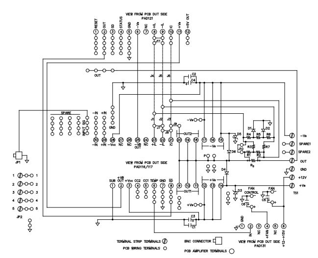
JUMPER SELECTION
Option 1: To use the PAD116/117 without fold-over current limit insert jumpers J1, 3, 7, 10 only (jumpers pre-installed for this option).
Option 2: To use the PAD116/117 with fold-over current limit insert jumpers J1, 2, 3 only.
Option 3: To use the PAD116/117 and PAD121 together without fold-over current limit insert jumpers J4, 6, 7, 8, 9, 10, 11 only.
Option 4: To use the PAD116/117 and PAD121 together with fold-over current limit insert jumpers J4, 5, 6, 7, 8, 9 only.
Refer to the PAD Power™ Excel spreadsheet (available for download from the website) for assistance in calculating resistor values for fold-over current limiting.
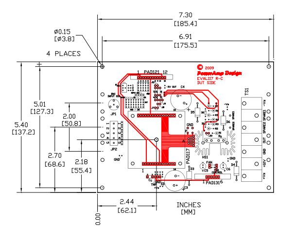
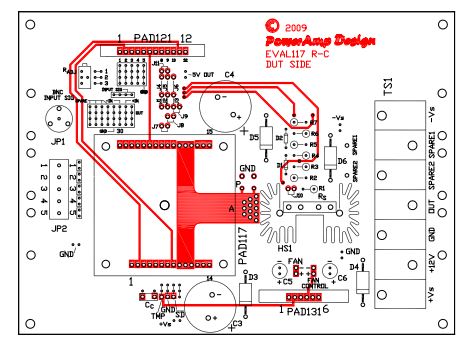
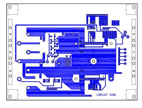
PCB VIEWS
TOP VIEW
BOTTOM VIEW
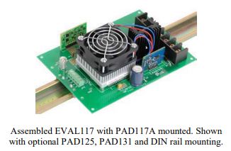
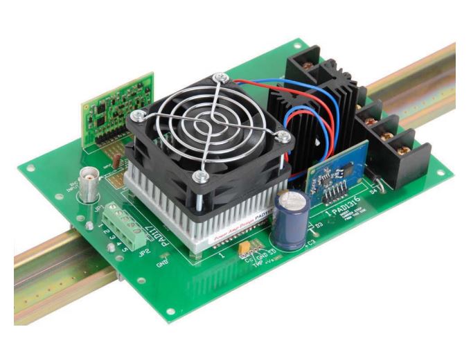
ASSEMBLED KIT
Assembled EVAL117 with optional DIN rail PCB mounting and PAD117 installed. Optional PAD121 and
PAD131 accessory modules are also shown.
DIMENSIONAL INFORMATION
BOARD OUTLINE DIMENSIONS