Downloads
Datasheet
PAD 146
Rev B
KEY FEATURES
- LOW COST
- POWER BANDWIDTH – 100kHz, 180Vp-p
- HIGH VOLTAGE – 200 VOLTS
- HIGH OUTPUT CURRENT – 20Apk
- 140 WATT DC DISSIPATION CAPABILITY
- 160 WATT AC DISSIPATION CAPACILITY
- WIDE SUPPLY RANGE ± 20V – ± 100V
- INTEGRATED HEAT SINK AND FAN
- TEMPERATURE REPORTING
- SHORT CIRCUIT PROTECTION
- OVER-TEMPERATURE SHUTDOWN
- CONFORMALLY COATED
RoHS COMPLIANT
APPLICATIONS
- PRINT HEAD PIEZO DRIVE
- SEMICONDUCTOR TESTING
- VIBRATION CANCELLATION
DESCRIPTION
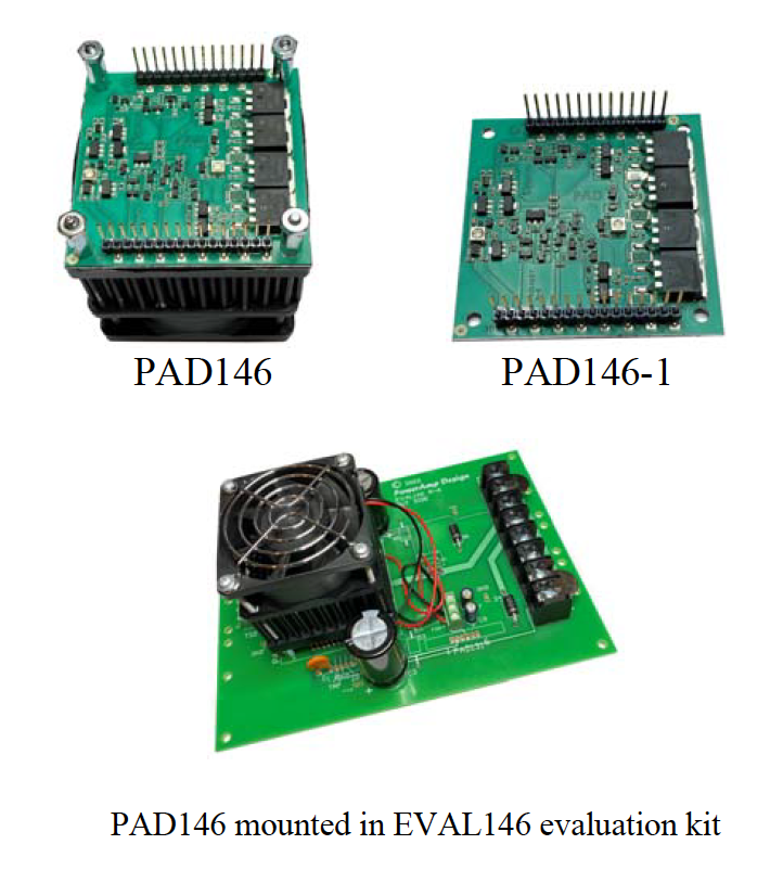
The PAD146 high power operational amplifier is constructed with surface mount components to provide a cost-effective solution for many industrial applications but is aimed primarily for driving industrial ink jet print heads. With a footprint only 5.6 in2 the PAD146 offers outstanding performance that rivals much more expensive hybrid components. User selectable external compensation tailors the amplifier’s response to the application requirements. The PAD146 also features a substrate temperature reporting output and over-temp and over-current shutdown. The amplifier circuitry is built on a thermally conductive but electrically insulating substrate mounted to an integral heat sink and fan assembly. No BeO is used in the amplifier. The resulting module is a small, high-performance turn-key solution for many industrial applications. For custom applications the PAD146-1 can be ordered without the heat sink and fan.
A NEW CONCEPT
A critical task in any power amplifier application is cooling the amplifier. Until now component amplifier manufacturers often treated this task as an after-thought, left for the user to figure out. At Power Amp Design the best heat sink and fan combination is chosen at the start and becomes an integral part of the overall amplifier design. The result is the most compact and volumetric efficient design combination at the lowest cost. In addition, this integrated solution concept offers an achievable real-world power dissipation rating, not the ideal rating usually cited when the amplifier case is somehow kept at 25oC. The user no longer needs to specify, procure or assemble separate components.
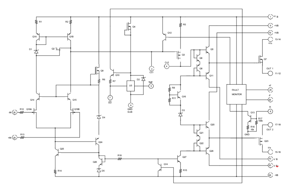
EQUIVALENT CIRCUIT
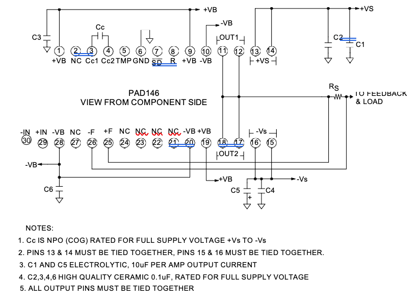
AMPLIFIER PINOUTS & CONNECTIONS
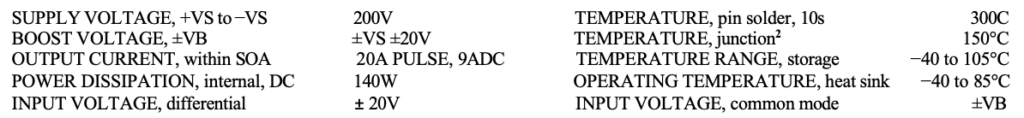
ABSOLUTE MAXIMUM RATINGS
| PARAMETER | TEST CONDITIONS1 | MIN | TYP | MAX | PAD146-19 | UNITS |
| INPUT | ||||||
| OFFSET VOLTAGE | 1 | 5 | mV | |||
| OFFSET VOLTAGE vs. temperature | Full temperature range | 20 | 50 | μV/OC | ||
| OFFSET VOLTAGE vs. supply | 20 | μV/V | ||||
| BIAS CURRENT, initial3 | 100 | pA | ||||
| BIAS CURRENT vs. supply | 0.1 | pA/V | ||||
| OFFSET CURRENT, initial | 50 | pA | ||||
| INPUT RESISTANCE, DC | 100 | G Ω | ||||
| INPUT CAPACITANCE | 4 | pF | ||||
| COMMON MODE VOLTAGE RANGE | +VB−12 | V | ||||
| COMMON MODE VOLTAGE RANGE | −VB+7 | V | ||||
| COMMON MODE REJECTION, DC | 98 | 106 | dB | |||
| NOISE | 100kHz bandwidth, 1kΩ RS | 10 | μV RMS | |||
| FAULT SENSING INPUTS | ||||||
| R (RESET), 10μS min pulse width | Relative to GND, >4.5V to insure reset | 0 | 5.5 | V | ||
| +F | -VB | +VB | V | |||
| -F | -VB | +VB | V | |||
| +F TO -F | Differential voltage, shutdown | ± 0.15 | V | |||
| SD | <0.2V to insure shutdown | 0 | 5.5 | V | ||
| GAIN | ||||||
| OPEN LOOP | RL= 10kΩ, CC=10pF | 108 | dB | |||
| GAIN BANDWIDTH PRODUCT @1MHz | CC=10pF | 10 | MHz | |||
| PHASE MARGIN | Full temperature range | 45 | 60 | degree | ||
| OUTPUT | ||||||
| VOLTAGE SWING | IO = 9A | +Vs−10 | +Vs−8.6 | V | ||
| VOLTAGE SWING | IO = −9A | −Vs+10 | −Vs+7 | V | ||
| VOLTAGE SWING | +VB= +Vs+10V, IO = 9A | +Vs−1.6 | +Vs−1.2 | V | ||
| VOLTAGE SWING | -VB= -Vs-10V, IO = -9A | -Vs+5.1 | -Vs+4.1 | V | ||
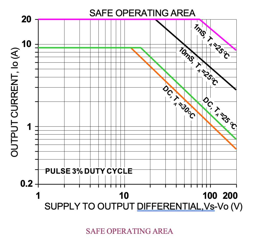
| CURRENT, continuous, DC | 9 | A | ||||
| SLEW RATE, AV = −10 | CC = 10pF | 65 | 85 | V/μS | ||
| SETTLING TIME, to 0.1% | 2V Step, CC = 10pF | 1 | μS | |||
| RESISTANCE | No load, DC | 4 | Ω | |||
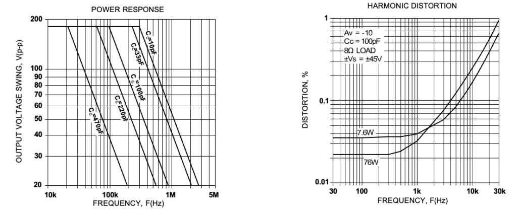
| POWER BANDWIDTH, 180Vp-p | CC = 10pF | 100 | kHz | |||
| POWER SUPPLY | ||||||
| VOLTAGE | ± 15 | ± 75 | ± 100 | V | ||
| CURRENT, quiescent | 27 | 33 | mA |
NOTES:
Unless otherwise noted: TC = 25OC, compensation Cc = 100pF, DC input specifications are ± value given, power supply voltage is typical rating.
Derate internal power dissipation to achieve high MTBF.
Doubles for every 10OC of case temperature increase.
4. +VS and −VS denote the positive and negative supply voltages to the output stage. +VB and −VB denote the positive and negative supply voltages to the input stages.
5. Rating applies if the output current alternates between both output transistors at a rate faster than 60Hz.
Power supply voltages +VB and −VB must not be less than +VS and −VS respectively. Total voltage +VB to −VB 240V maximum.
The PAD146 is constructed with MOSFET transistors and ESD handling procedures must be observed.
| PARAMETER | TEST CONDITIONS | MIN | TYP | MAX | PAD146-1 | UNITS |
| THERMAL | ||||||
| RESISTANCE, AC, junction to air5 | Full temperature range, f ≥ 60Hz | 0.78 | 0.4 | OC/W | ||
| RESISTANCE, DC, junction to air | Full temperature range | 0.89 | 13 | OC/W | ||
| RESISTANCE, DC, junction to case | 0.5 | |||||
| TEMPERATURE RANGE, heat sink | −40 | 85 | NA | OC | ||
| TEMPERATURE RANGE, substrate | 105 | |||||
| TEMPERATURE RANGE, ambient | 85 | NA | ||||
| FAN, 60mm dc brushless, ball bearing | ||||||
| OPERATING VOLTAGE | 12 | NA | V | |||
| OPERATING CURRENT | 150 | NA | mA | |||
| AIR FLOW | 25 | NA | CFM | |||
| RPM | 3800 | NA | RPM | |||
| NOISE | 30 | NA | dB | |||
| L10, life expectancy, 50OC9 | 45 | NA | kHrs | |||
| L10, life expectancy, 25OC9 | 60 | NA | kHrs |
5. Rating applies if the output current alternates between both output transistors at a rate faster than 60Hz.
9. L10 refers to the time it takes for 10% of a population of fans to fail.
SAFETY FIRST
The operating voltages of the PAD146 are potentially deadly. When developing an application circuit, it is wise to begin with power supply voltages as low as possible while checking for circuit functionality. Increase supply voltages slowly as confidence in the application circuit increases. Always use a “hands off” method whereby test equipment probes are attached only when power is off.
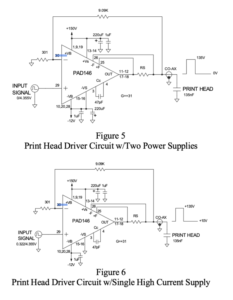
PRINT HEAD APPLICATIONS
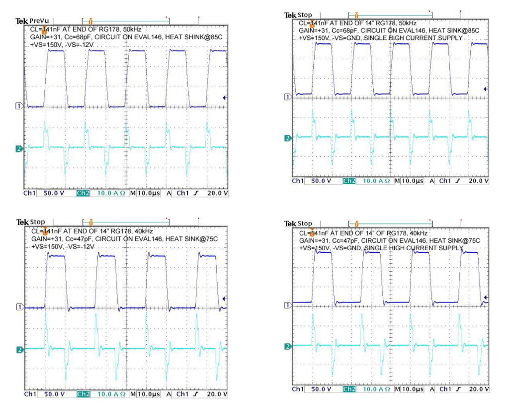
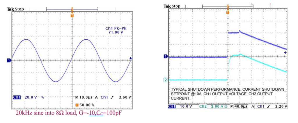
Although the PAD146 can be used for many applications it is primarily intended for ink jet print head driver applications. It can drive large pulse currents at high frequencies into the capacitive load of an ink jet print head. The various protection features of the PAD146 are ideal for such an application. The PAD146-1 version is available without the heat sink and fan for custom applications where the user supplies a customheat sink. In addition, the PAD146 is conformally coated for operation in challenging environments. You can find suggested circuits (Figures 5 and 6) on page 12 and the resulting o’scope photos at the top of page 9.
OVER-CURRENT FAULT PROTECTION
The output stage of the PAD146 is shut down when an over- current fault is detected. The protection circuit monitors the voltage across an external sense resistor, RS. The fault condition set point is programmed by:
IF= 0.15V/RS
Where IF is the value of the fault current set point and RS is the value of the sense resistor. Whenever the programmed current set point is exceeded for more than 10µS (typical) the drive to the output stage turns off (typically in less than 200µS), and remains off until the circuit is reset (pin 8, R) via a 5V momentary pulse ≥ 10µS (or power recycled). The internal sense voltage reference is a precision temperature compensated reference voltage of 0.15V. The accuracy of the current fault sensing is typicallybetter than 2%, plus the tolerance of the external sense resistor. A Kelvin sense resistor is recommended for best accuracy, but a properly connected standard resistor usually suffices. For some loads a start-up current may exceed the normal programmed maximum value. This condition should be considered when setting the programmed fault value. See Figure 1, below, for a typical over-current fault connectiondiagram. Note that during 10µS it takes to initiate shutdown the current may still be increasing depending on the details of the application. The sense resistor must be a very low inductance type with sufficient pulse power capability. A surface mount resistor is recommended of the type WFMA available from Vishay Dale. Several full part numbers are available in the parts list of the EVAL146 datasheet.
TEMPERATURE REPORTING
An analog output voltage is provided (pin 5, TMP) relative to ground (PIN 6) and proportional to the temperature in degreesC. The slope is approximately -10.82mV/oC. The output voltage follows the equation:
T = (2.127 ─ V) (92.42)
or
V = 2.127 ─ (T/92.42)
Where V is the TMP output voltage and T is the substrate temperature in degrees C.
SHUTDOWN FUNCTIONS
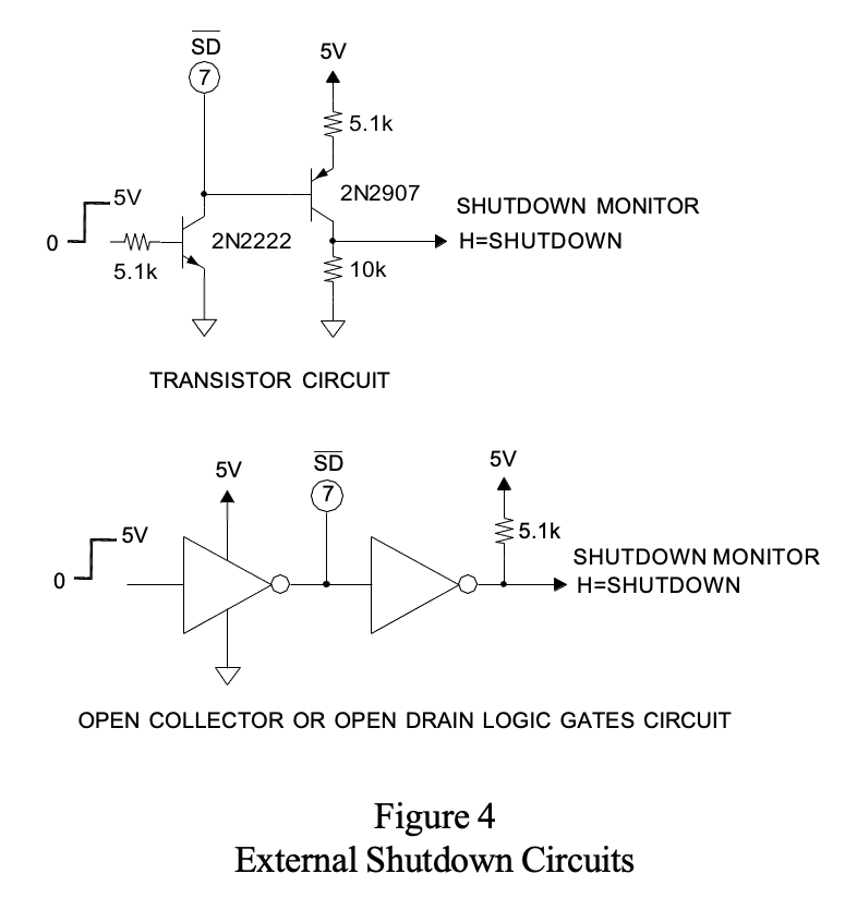
The temperature monitoring circuit automatically turns off the output MOSFETs when the substrate temperature reaches 110oC. The output remains disabled until the substrate temperature falls below 100oC and the circuit is reset (R, pin 8). The thermal shutdown feature is activated by amplifier thermal overload such as sustained high-power dissipation or inadequate heat sinking. The PAD146 may also be shut down using the SD function at pin 7. When pin 7 is driven low (to ground) the output of the amplifier shuts off (the output stage can supply no significant current but it is not a high impedance as some small current may still be available at the output pins and the output voltage during shutdown will be determined by the external circuit). Pin 7 may also serve as a monitor of the amplifier’s status. When pin 7 is monitored with a high impedance circuit a “high” at pin 7 (about 5V) will indicate that the amplifier is functioning normally. A “low” (about ground voltage) will indicate that the amplifier is in its shutdown mode. When reset is applied the amplifier will resume normal operation unless the fault is still present. A continuous “high” at the reset pin will disable the fault circuits and consequently a reset signal should only be applied as a short pulse. See Figure 4 in Applications, page 11, for external shutdown circuits.

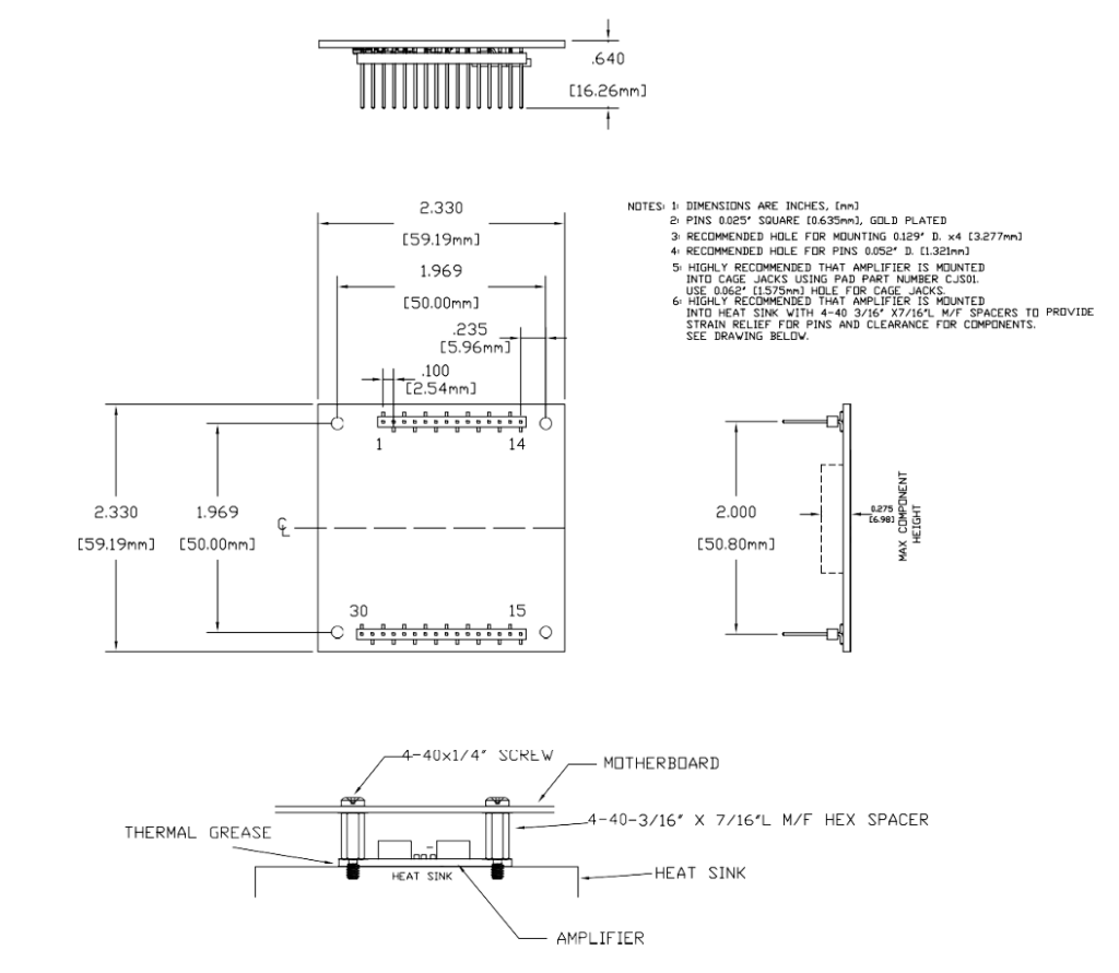
MOUNTING THE PAD-146-1
In most applications the PAD146-1 must be attached to a heat sink. Spread a thin and even coat of heat sink grease across the back of the PAD146-1 and also the heat sink where the amplifier is to be mounted. Push the amplifier into the heat sink grease on the heat sink while slightly twisting the amplifier back and forth a few times to bed the amplifier into the heat sink grease. On the final twist align themounting holes of the amplifier with the mounting holes in the heat sink and finish the mounting using 4-40 X 3/16” X 7/16” hex male-female spacers. Mount the amplifier to the mother board with 4-40 X 1/4” screws.
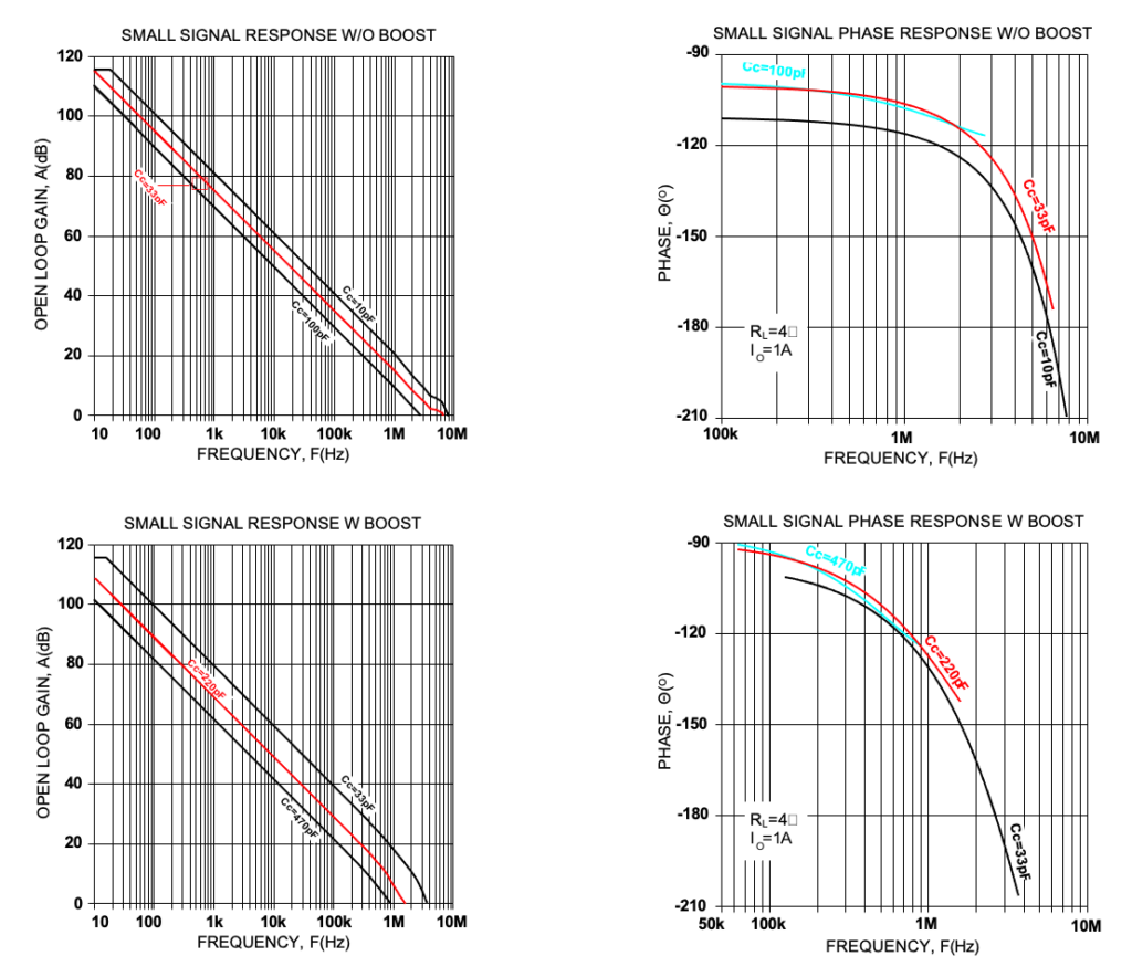
PHASE COMPENSATION
The PAD146 must be phase compensated. The compensation capacitor, CC, is connected between pins 3 and 4. The compensation capacitor must be an NPO type capacitor rated for the full supply voltage (200V). Consult also the small signal response and phase response plots for the selected compensation value in the Typical Performance Graphs section. Do not use a compensation capacitor less than 10pF. Recommended starting compensation capacitor, Cc, is 100pF.
BOOST OPERATION
The small signal stages of the PAD146 are connected to the ±VB power supply pins. When the ±VB voltages are greater than the ±VS power supply pins by 10V or more the small signal stages of the amplifier are biased so that the output MOSFETs can be driven very close to the ±VS rails. Close swings to the supply rails increase the efficiency of the amplifier and make better use the supply voltages. This technique is often used to operate the amplifier with only a single high current power supply, thus reducing the system size and cost. Also see the application article AN-22 Single Supply Operation with Power Op Amps for more detailed information and circuits. However, best fidelity of the output signal and highest frequency response is achieved when the output signal does not approach the power supply rails by less than 10V.
CONFORMAL COATING
The PAD146 has a conformal coating to help protect against humidity and dirty environments. It is best that the circuit only be handled by the edges of the board to prevent disturbing the coating.
BOARD LAYOUT CONSIDERATIONS
The PAD146 can produce 20A pulse currents with a rise time of 1μS or less. Therefore, power supply bypassing and parasitic inductance are very important design considerations. All of the power supply pins (1, 9, 10, 13-14, 15-16, 19, 20, 28) should be bypassed with a 1μF ceramic capacitor placed physically very close to the power supply pins. The board traces leading to these pins should be wide to lower inductance (minimum of 0.035”) The ground system should be a ground plane and in particular the ground connection of the substrate (pin 6) needs to be connected to the ground plane with a very short and wide trace. In addition to the ceramic bypass capacitors a large electrolytic capacitor of 220-470μF needs to be connected to each of the high current power supply pins (13-14 and 15-16). These capacitors also need to be placed physically very close to the power supply pins. Likewise the board traces connecting the output pins and the co-ax cable should also be wide (at least 0.15”) and 2oz Cu. It is recommended that the print head be connected to the amplifier with co-ax cable (RG178, for example). An examination of the layout of the EVAL146 board will illustrate these requirements for a successful application board.
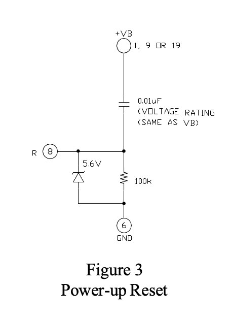
POWER UP CONDITIONS
In most applications the PAD146 is powered by two power supplies. Under normal conditions both power supply voltages start to ramp up totheir final values at the same time. However, if one power supply starts well before the other the over-current protection circuit may keep the output stage turned off. In this case it will be necessary to apply a momentary 5V reset pulse to pin 8 (Reset) to unlock the output stage of the amplifier. An auto-reset circuit can be connected to pin 8 to ensure that the amplifier’s output is active upon power up, although this is not necessary if the power supplies are started at the same time. The form of this circuit is shown in Figure 3, Applications, page 11.
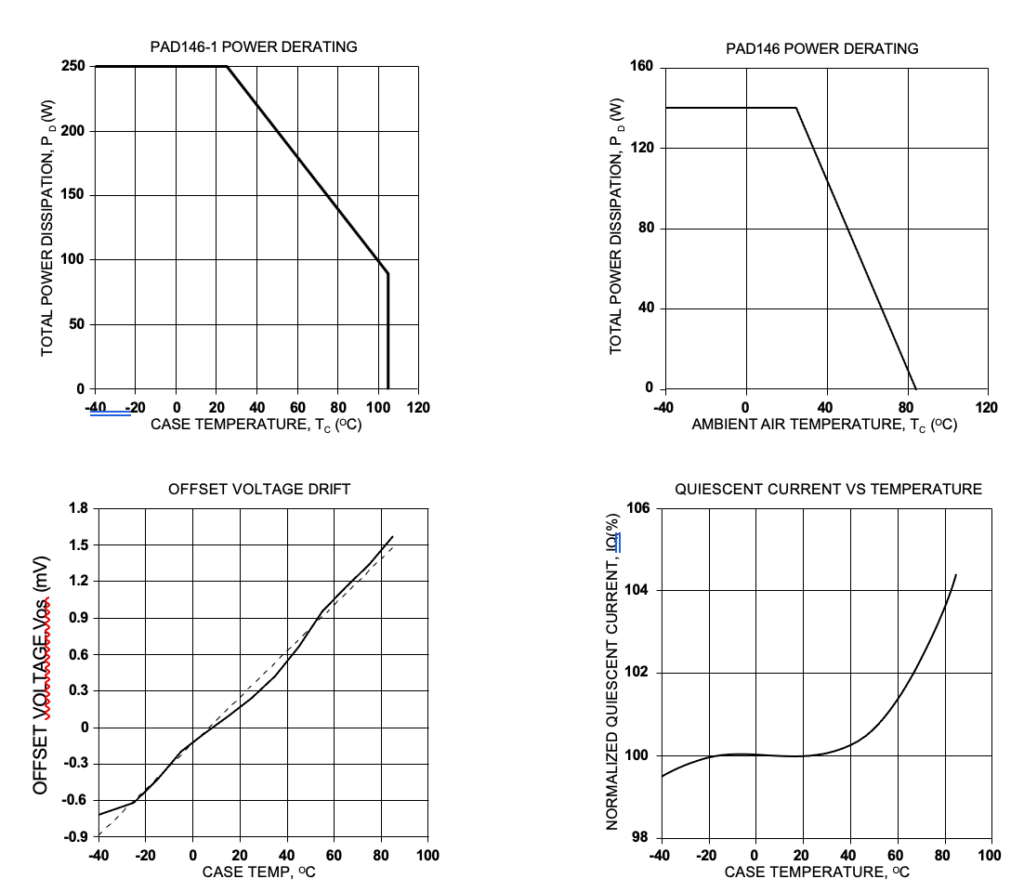
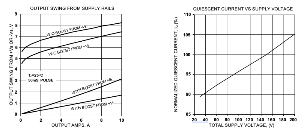
TYPICAL PERFORMANCE GRAPHS
DIMENSIONAL INFORMATION