Downloads
Datasheet
PAD148 – Rev K
KEY FEATURES
- LOW COST
- HIGH VOLTAGE – 200 VOLTS
- HIGH CURRENT – 10 AMPS
- 125 WATT DISSIPATION CAPABILITY
- 100kHz POWER BANDWIDTH
- SHORT CIRCUIT PROTECTION
- TEMPERATURE MONITORING
- RoHS COMPLIANT
- CONFORMALLY COATED
APPLICATIONS
- INKJET PRINTER HEAD DRIVE
- PIEZO TRANSDUCER DRIVE
- INDUSTRIAL INSTRUMENTATION
- RELECTOMETERS
- ULTRA-SOUND TRANSDUCER DRIVE
DESCRIPTION
The PAD148-1 is a high voltage operational amplifier constructed with surface mount components to provide a cost effective solution for many industrial applications With a footprint only
3.3in2 the PAD148-1 offers outstanding performance that rivals more expensive hybrid component amplifiers. User selectable external compensation tailors the amplifier’s response to the application requirements. An analog output voltage is provided that is proportional to the substrate temperature. The amplifier’s output stage is shut down by pulling the shut down pin low or when the substrate temperature exceeds 110oC. A short circuit or over-current condition also shuts down the output stage. The amplifier circuitry is built on a thermally conductive but electrically insulating substrate. No BeO is used in the PAD148-1. The resulting module is a small, high performance solution for many industrial applications. The PAD148-1 is a special version of the base product PAD148 where the fault sense voltage is 0.65V and the output stage is biased class C to lower quiescent current.
PAD148-1
CIRCUIT & CONNECTIONS
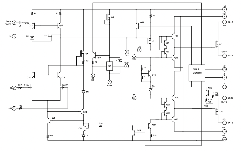
EQUIVALENT CIRCUIT
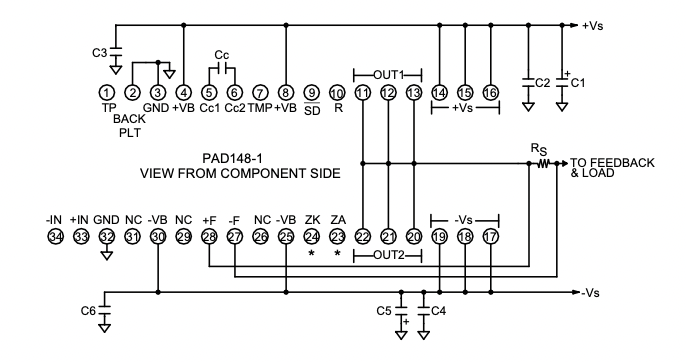
PINOUT & CONNECTIONS
NOTES:
- Cc IS NPO (COG) RATED FOR FULL SUPPLY VOLTAGE +Vs TO -Vs
- PINS 4 & 8 MUST BE TIED TOGETHER. PINS 25 & 30 MUST BE TIED TOGETHER.
- C1 AND C5 ELECTROLYTIC, 10uF PER AMP OUTPUT CURRENT
- C2,3,4,6 HIGH QUALITY CERAMIC 0.1uF
- ALL OUTPUT PINS MUST BE TIED TOGETHER
* *MAKE NO CONNECTION FOR PAD148-1
ABSOLUTE MAXIMUM RATINGS
NOTES:
- Unless otherwise noted: TC = 25OC, compensation Cc = 100pF, DC input specifications are value given, power supply voltage is typical rating.
- Derate internal power dissipation to achieve high MTBF.
- Doubles for every 10OC of case temperature increase.
- +Vs and −Vs denote the positive and negative supply voltages to the output stage. +VB and −VB denote the positive and negative supply voltages to the input stages.
- Rating applies if the output current alternates between both output transistors at a rate faster than 60Hz.
- Power supply voltages +VB and −VB must not be less than +Vs and −Vs respectively. Total voltage +VB to −VB 240V maximum.
- The PAD148-1 is constructed with MOSFET transistors and ESD handling procedures must be observed.
SAFETY FIRST
The operating voltages of the PAD148-1 are potentially deadly. When developing an application circuit it is wise to begin with power supply voltages as low as possible while checking for circuit functionality. Increase supply voltages slowly as confidence in the application circuit increases. Always use a “hands off” method whereby test equipment probes are attached only when power is off.
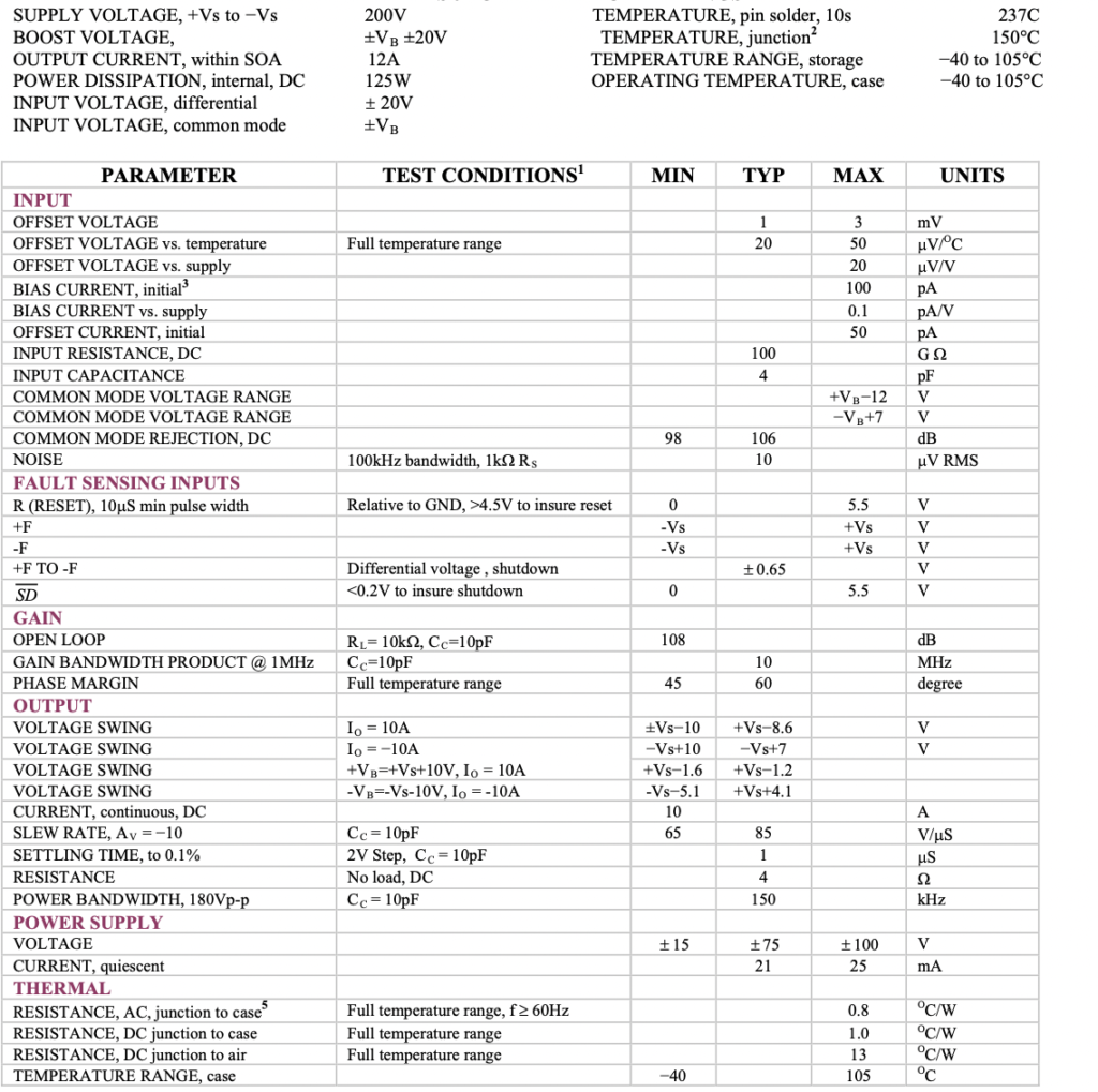
OVER-CURRENT FAULT PROTECTION
The output stage of the PAD148-1 is shut down when an over-current fault is detected. The protection circuit monitors the voltage across an external sense resistor, Rs. The fault condition set point is programmed by:

Whenever the programmed current set point is exceeded for more than 10 μS (typical) the drive to the output stage turns off completely (typically in less than 400μS), and remains off until the circuit is reset (pin 10, R) via a 5V momentary pulse ≥ 10μS (or power recycled). The internal sense voltage is a precision temperature compensated reference voltage of 0.65V. The accuracy of the current fault sensing is typically better than 2%, plus the tolerance of the external sense resistor. A Kelvin sense resistor is recommended for best accuracy. For some loads a start-up current may exceed the normal programmed maximum value. This condition should be considered when setting the programmed fault value. See Figure 1, below, for a typical over-current fault connection diagram.
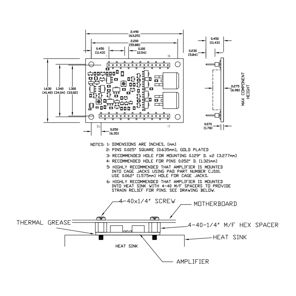
MOUNTING THE AMPLIFIER
In most applications the amplifier must be attached to a heat sink. Spread a thin and even coat of heat sink grease across the back of the PAD148-1 and also the heat sink where the amplifier is to be mounted. Push the amplifier into the heat sink grease on the heat sink while slightly twisting the amplifier back and forth a few times to bed the amplifier into the heat sink grease. On the final twist align the mounting holes of the amplifier with the mounting holes in the heat sink and finish the mounting using 4-40 hex male-female spacers. Mount the amplifier to the mother board with 4-40 X 1/4” screws.
PHASE COMPENSATION
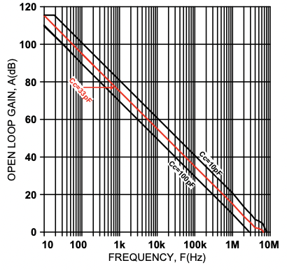
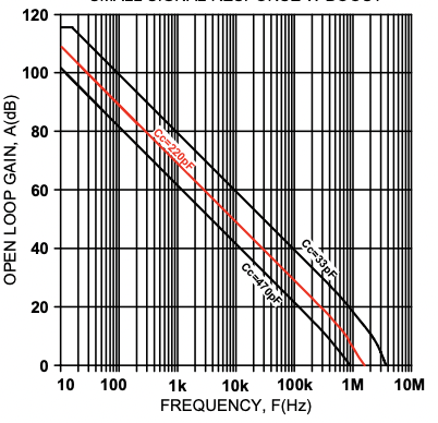
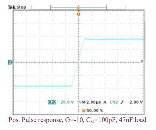
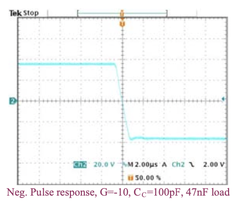
The PAD148-1 must be phase compensated. The compensation capacitor, CC, is connected between pins 5 and 6. The compensation capacitor must be an NPO type capacitor rated for the full supply voltage (200V). On page 2, under Amplifier Pinout and Connections, you will find a table that gives recommended compensation capacitance value for various circuit gains and the resulting slew rate for each capacitor value. Consult also the small signal response and phase response plots for the selected compensation value in the Typical Performance Graphs section. Do not use a compensation capacitor less than 10pF.
BOOST OPERATION
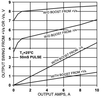
The small signal stages of the PAD148-1 are connected to the ±V B power supply pins. When the ±V B voltages are greater than the ±Vs power supply pins the small signal stages of the amplifier are biased so that the output transistors can be driven very close to the ±Vs rails. Close swings to the supply rails increase the efficiency of the amplifier and make better use the supply voltages. This technique is often used to operate the amplifier with only a single high current power supply, thus reducing the system size and cost. Also see the application article AN-22 Single Supply Operation with Power Op Amps for more detailed information and circuits.
TEMPERATURE REPORTING
An analog output voltage is provided (pin 7, TMP) relative to ground (PIN 3) and proportional to the temperature in degrees C. The slope is approximately -10.82mV/oC. The output voltage follows the equation:
T = (2.127 ─ V) (92.42)
or
V = 2.127 ─ (T/92.42)
Where V is the TMP output voltage and T is the substrate temperature in degrees C.
THERMAL SHUTDOWN
The temperature monitoring circuit automatically turns off the output transistors when the substrate temperature reaches 110oC. The output remains disabled until the substrate temperature falls below 100 oC and the circuit is reset (R, pin 10). The thermal shutdown feature is activated by amplifier thermal overload such as sustained high power dissipation or inadequate heat sinking.
EXTERNAL SHUTDOWN
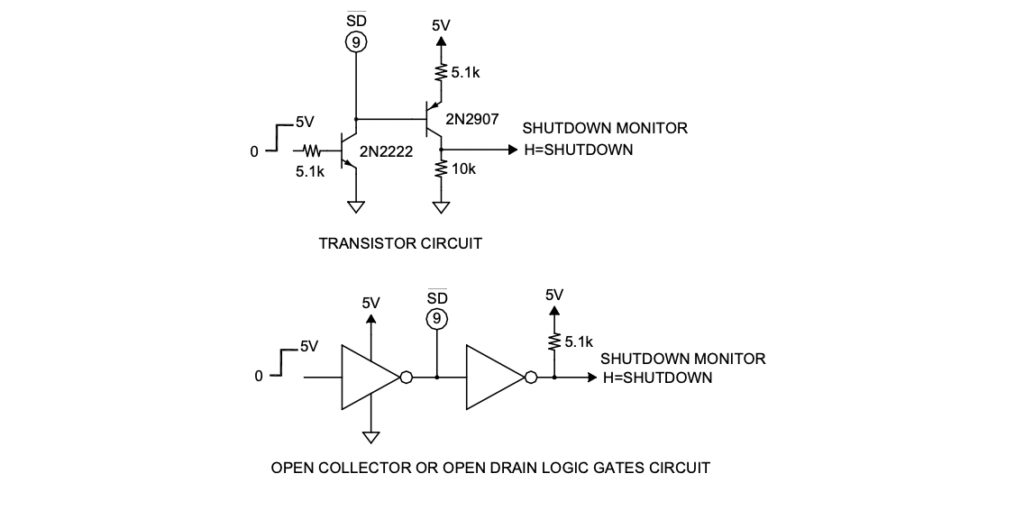
When pin 9 (SD) is taken low (GND) the output stage is turned off and remains off until reset at pin 10 (R) with a 5V pulse or power to the amplifier is restarted. If the SD pin is monitored with a high impedance circuit (>100k input impedance) it also gives an indication of the temperature status of the amplifier. A “high” (+5V) indicates normal temperature operation and a “low” (zero volts, approximately) indicates that the amplifier is shut down due to the occurrence of an over- temp condition. See Figure 4 in Applications, page 10, for external shutdown circuits.
POWER-UP CONDITIONS
In most applications the PAD148-1 is powered by two power supplies. Under normal conditions both power supply voltages start to ramp up to their final values at the same time. However, if one power supply starts well before the other the over-current protection circuit may keep the output stage turned off. In this case it will be necessary to apply a momentary 5V reset pulse to pin 10 (Reset) to unlock the output stage of the amplifier. A auto-reset circuit can be connected to pin 10 to ensure that the amplifier’s output is active upon power up, although this is not necessary if the power supplies are started at the same time. The form of this circuit is shown in Figure 3, Applications, page 10.
CONFORMAL COATING
The PAD148-1 has a conformal coating to help protect against humidity and dirty environments. It is best that the circuit only be handled by the edges of the board to prevent disturbing the coating. The silicone conformal coat is Dow Corning 1-2577 and is applied in a thickness from 0.1 to 0.2 mm.
TYPICAL PERFORMANCE GRAPHS
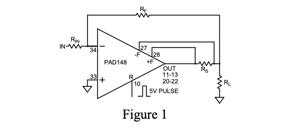
POWER DERATING
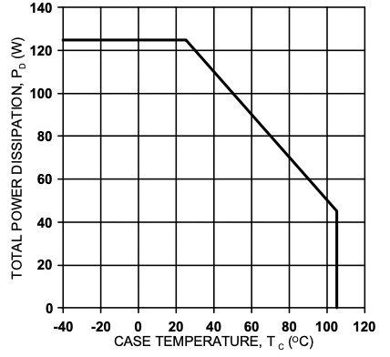
OFFSET VOLTAGE DRIFT
OUTPUT SWING FROM SUPPLY RAILS
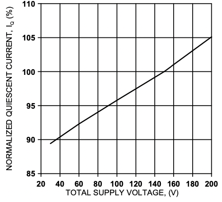
QUIESCENT CURRENT VS SUPPLY VOLTAGE
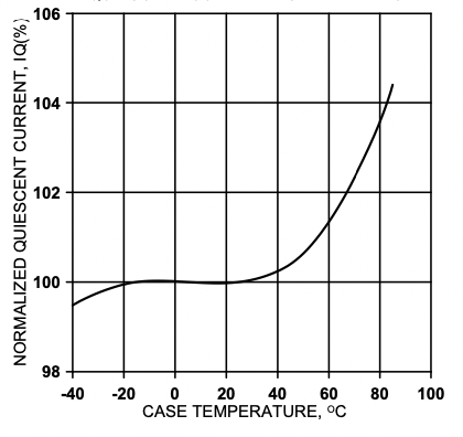
QUIESCENT CURRENT VS TEMPERATURE
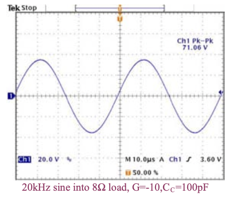
TYPICAL PERFORMANCE GRAPHS
SMALL SIGNAL RESPONSE W/O BOOST
SMALL SIGNAL RESPONSE W BOOST
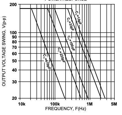
POWER RESPONSE
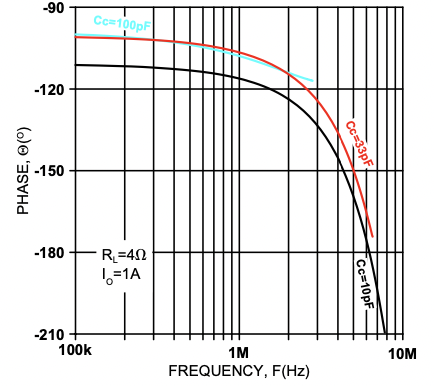
SMALL SIGNAL PHASE RESPONSE W/O BOOST
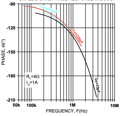
SMALL SIGNAL PHASE RESPONSE W BOOST
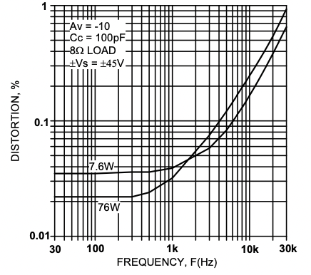
HARMONIC DISTORTION
TYPICAL PERFORMANCE GRAPHS
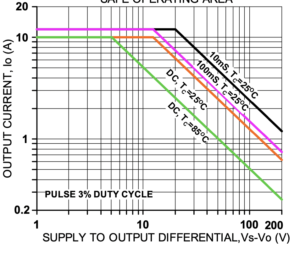
SAFE OPERATING AREA
APPLICATION CIRCUITS

Power-up Reset
External Shutdown Circuits
DIMENSIONAL INFORMATION