Power Op Amp
Application Notes Library
V1.1
Introduction to the Power Op Amp Application Library V1.0
Most electronic engineers today have had at least a little training with operational amplifier circuits. College courses, for example, instruct us how to calculate gain and accuracy of many of the standard op amp circuits. But power op amp circuits are a little different. While power op amps operate on the same principles as IC op amps, power op amp circuits are meant for different applications. IC op amp circuits are mainly aimed at manipulating analog information whereas power op amps circuits usually are meant to drive transducers of some sort (motors, piezo elements, etc.). And while the circuit basics are the same as IC op amps, power op amps have many specialized variations and circuit layout considerations.
This compilation of the application notes from Power Amp Design expand on the individual model datasheets of our products and guide the engineer with proven circuits and methods for successfully applying power op amp circuits.
AN-10
The Rail to Rail Advantage
Power Amp Design
Synopsis: Examples are given to illustrate the technical advantages for a power operational amplifier whose output voltage can closely approach the power supply voltages both for dual and single supply applications. Supporting calculations are given using a dedicated spreadsheet that can be downloaded from the internet.
In recent years the small-signal monolithic rail to rail input, rail to rail output, operational amplifier has become a mainstay in the arsenal of several manufacturers’ amplifier lines. These op amps go by the moniker of RRIO op amps and are usually powered by 5 volts. They can be operated with the inputs biased to either supply rail and the outputs can approximate the power supply rails with light loading (micro-amps to a few milliamps). The impetus for this kind of design is simple enough: in many applications the few volts of available supply voltage needs to result in the largest possible output signal amplitude and not squandered on “drop from the rail” that reduces the maximum peak to peak output signal that conventional op amp designs exhibit. The RRIO design can produce almost 5VP-P of usable output signal with only a 5V supply. Also, with an input common mode range capable of reaching the negative supply rail (ground, most often) the amplifier can be operated with a single (5V) supply.
In the world of power op amps things are a little different. Power op amps usually operate with much higher supply voltages, far more output current and can deliver tens or hundreds of watts to a load. The impetus to design a RRIO power op amp is similar even though the supply voltages and output currents are far greater than with its monolithic cousins.
For a RRIO power op amp efficiency is the prime design motivator. Even when power supply voltages are far higher than 5V the ability for the output to swing very close to the supply voltage is important. Let’s look at an example of the advantage of the model PAD117 RRIO power op amp from Power Amp Design vs. a conventional power op amp design. Consider Figure 1below. To calculate critical parameters such as the amplifier’s output transistor junction temperature and the amplifier’s case temperature we will use the PAD Power spreadsheet available for download from website.
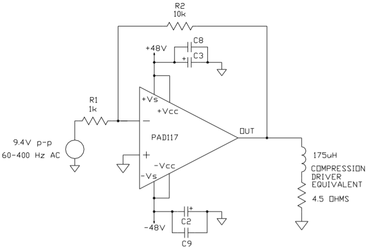
Load: compression driver, 4.5Ω, 175µH, operating @ 60-400Hz
Supply: ±48V
Full output: 94VP-P. (+47V to -47V, only 1V from each supply rail required to produce 10.4A peak into the load)
Ambient temperature: 30°C
Using the PAD Power spreadsheet we find that:
Output amps peak=10.4A
Output VRMS=33.2V
Amplifier case temperature=83.7°C
Maximum output transistor temperature=126.4°C
Amplifier dissipates 103.7WRMS
Amplifier delivers 245.4WRMS to the load
For another amplifier without rail to rail output capability (but otherwise equal to the PAD117) the internal biasing necessary to operate the output transistor will typically require a 6V drop from the rail to deliver 10.4A to the load. To get the same 94VP-P voltage to the transducer the supply voltage necessary is ±53V (47Vpeak + 6V from each power supply rail). With the same output volts and amps to the load the conventional amplifier design will now need to tolerate:
Amplifier case temperature=95.3°C
Maximum output transistor temperature=147.3°C
Amplifier dissipates 126.5WRMS
The following table summarizes the analysis results:
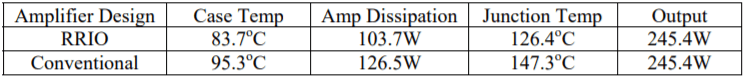
From this example we can see that while the PAD117 RRIO op amp operates comfortably with this load. A similar design without rail to rail output operation operates at noticeably higher output transistor junction temperature and amplifier case temperature due the lower operating efficiency. Using the data from the table we can calculate that the conventional amplifier design dissipates 22% more power while delivering the same output power.
This example was constructed to illustrate the efficiency advantage of a RRIO amplifier, but also other points as well: You will not find a commercial power op amp capable of a case temperature 95°C or a 100V amplifier that is allowed to operate on ±53V (106 V total). To solve the first problem you would need to purchase a military grade amplifier so that a 95°C case temperature is permitted. To solve the second problem you would need to find an amplifier rated at more than 100V of total supply voltage (200V is the next rating step). Both of these solutions are much more expensive. For cost reasons the only practical solution is to lower the power supply voltages so that the operating voltage of the amplifier will not be exceeded. Additionally, the power supply voltage must be reduced enough to bring down the amplifier case temperature to a commercial rating of 85°C or less. Lowering the power supply voltages also lowers the power that can be delivered to the load.
In this example reducing the power supply voltages from ±53V to ±48V and reducing the output signal solves the problem. Again, using the PAD Power spreadsheet, the operating parameters are:
Ambient temperature: 30°C
Supply: ±48V
Full output: 88VP-P.
Output amps peak = 9.8A
Output VRMS=31.1V
Amplifier case temperature=83.7°C
Maximum output transistor temperature=126.4°C
Amplifier dissipates 103.7WRMS
Amplifier delivers 215.1WRMS to the transducer
The following table summarizes the performance of the RRIO amplifier design and the modified conventional amplifier design:
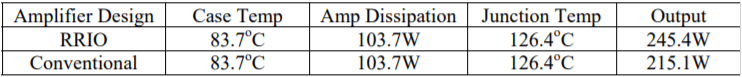
In this example while the PAD117 RRIO op amp can deliver 245.4WRMS to the load a conventional amplifier design under the same conditions can only deliver 215.1WRMS to the load. Stated another way, under these conditions the PAD117 can deliver 14.1% more power to the load while dissipating the same power as a conventional amplifier design.
It’s important to further note that as the power supply voltage decreases the relative advantage of the RRIO amplifier increases. This is simply because as the power supply voltage decreases the voltage drop from the rail of the conventional design increases much more rapidly as a proportion of the available voltage from the power supply than with the RRIO design.
Figure 2 shows one way to take full advantage of the RRIO amplifier by using its rail to rail features at both the input and output of the amplifier. In the example only one 36V power supply is required. E1 generates the peak to peak signal that will be gained a factor of 10 by the amplifier. E2 provides an offset of +17.5V so that the output of the amplifier will swing symmetrically from +35 to 0 volts at its output.
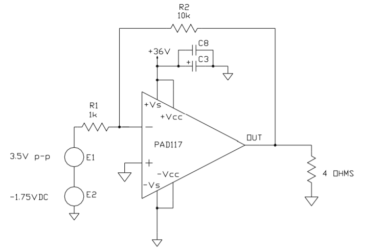
It is, of course, possible to operate a conventionally designed power op amp with one power supply. Since the power supply is the single most expensive component in an application circuit (other than the amplifier and load device) operating with only one power supply is a considerable economic advantage. But compared to a conventional op amp design the RRIO amplifier has two significant additional advantages in this circuit. As shown in the first example the output of the RRIO amplifier can swing much closer to the supply voltage than the conventional amplifier. But, in addition, the RRIO amplifier can actually reach zero volts at its output when there is no current in the load. A conventional amplifier design cannot reach zero output volts even when there is no load current. A typical no-load output voltage for the conventional amplifier operated with a single supply is about 2-5V. With a single 36V supply the PAD117 can achieve a 35VP-P into the load. A conventional amplifier could only achieve about 25-28 VP-P. In addition, the PAD117 has a common mode voltage range that includes ground for single supply applications. The non-inverting input can be grounded, thus avoiding a messy biasing scheme that the conventional amplifier design would require to bias its non-inverting input at some voltage above ground (usually in the range of 5-15V).
The advantages of the rail to rail amplifier, then, are many. The ability to operate on a single supply saves the cost of an additional power supply (and the cost and space of the associated by-pass capacitors). The operating efficiency is significantly higher due to its low voltage drop from the supply rail. That efficiency also results in lower operating costs and lower amplifier operating temperatures that enhance reliability. And its ability to operate with a common mode input voltage to ground with single supply operation aids in the design of simple input circuits.
AN-12
The Problem with Current Limit
Power Amp Design
Synopsis: Traditional current limiting circuits may not offer the operational amplifier the protection it needs to be reliable in an application circuit. The problems associated with one traditional current limiting circuit are analyzed and a new solution is explained featuring the PAD121 Current Limit Accessory module offered by Power Amp Design.
Pick most any monolithic op amp available and you will undoubtedly see specifications for maximum output current and short circuit current. The output current is most often limited by a simple transistor circuit that senses the drop across a small value resistor in the output path and this transistor circuit tugs on the drive to the output transistor to prevent it from supplying too much current. See Figure 1. The idea is to protect the amplifier from overheating that may destroy the op amp.
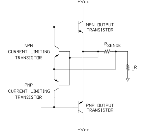
The advantages of this current limiting circuit are that few components (2 transistors and a sense resistor) are involved, the components don’t take up much area on the monolithic chip and therefore the circuit is cheap.
The most serious disadvantage of this circuit is that it doesn’t necessarily protect the amplifier. What usually destroys an amplifier is not the output current directly, but the power dissipation the amplifier must withstand while current limiting. More about this important point later.
And there are other disadvantages as well:
The circuit is not very accurate; a 20% or 30% tolerance can be expected. The wide tolerance means that the current limit must be set at least that much above the current level that is expected in normal operation.
The circuit is temperature sensitive. As the temperature of the amplifier rises the calculated trip point for current limit will decrease about .3%/°C. This also requires that the current limit set point be raised to accommodate the expected current at the maximum operating temperature.
The circuit may be non-symmetrical. Both NPN and PNP transistors are used in the circuit, the NPN to sense positive current and the PNP to sense negative current. The positive and negative current limit set points will follow the Vbe of the NPN and PNP transistors. The Vbe of these opposite sex transistors are usually not equal and that results in non-symmetric current limit trip points.
The sense voltage is approximately 0.6V-0.7V, the Vbe of a typical bipolar transistor. This voltage reduces the maximum output swing of the amplifier. Perhaps worse yet, amplitude of sense voltage can produce significant power dissipation in the current limit sense resistor when this technique is applied to power op amps. A 5-10W dissipation in the sense resistor for a power op amp circuit is not uncommon.
Now to address this circuit’s most serious flaw—that it does not necessarily protect the amplifier. Notice that once the amplifier has entered current limit the function of the op amp circuit shifts to that of a constant current amplifier. As far as the safety of the op amp is concerned this is dangerous territory. Consider Figure 2.
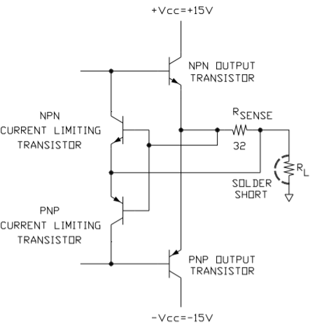
The output of the monolithic op amp has been shorted to ground by a solder bridge. The current limit has been set to 20mA. The NPN output transistor now has 14.4V across it while conducting 20mA. The resulting power dissipation in the output transistor is 288mW. Perhaps, instead, the solder bridge connects the output to the negative supply voltage. Now there is 588mW in the NPN output transistor. Will the monolithic op amp survive? Maybe yes, maybe no.
Let’s move away from the monolithic op amp and up a notch to the power op amp. Consider Figure 3.
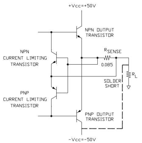
The supply voltages are +/- 50V and a similar current limit circuit is used and is set to trip at 7A. Just as in the example with the monolithic op amp let’s suppose a solder bridge has shorted the output to the negative supply voltage. The NPN output transistor of the power op amp now must dissipate 700W in order to survive. It won’t! Very shortly a puff of smoke may signal the end of the trail for this op amp.
One technique that helps protect the amplifier is dual slope current limit (fold-over current limit). As the voltage across the output transistor increases beyond some point the current limit value is reduced, thus helping the amplifier survive over-current conditions. See Figure 4.
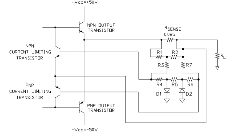
This is an improved current limiting technique but it does not eliminate the other disadvantages mentioned previously. The details of the operation of fold-over current limiting will not be discussed here but Power Amp Design has help available. See below.
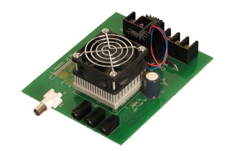
A new technique developed by Power Amp Design in the PAD121 Current Limit Accessory Module advances the protection of power op amps. The problems of the old current limit circuit scheme have been reduced or eliminated by this external circuit.
The PAD121 addresses the limitations of the old current limit circuits by providing a host of new features:
The sense voltage has been reduced from the 0.6V-0.7V of the old circuit technique to a precision 150mV. Moreover, the sense voltage is temperature stable. The lower sense voltage reduces the power dissipation in the sense resistor to 25% or less of that with the old current limit technique. Three connections for the current limiting circuitry are brought out so that both 4-wire and fold-over current limiting can be implemented. Power Amp Design has developed a spreadsheet called PAD Power™ that calculates the values of the resistors for the fold-over current limit technique as seen in Figure 4 as well as many other design solutions. PAD Power™ can be downloaded from the website.
Whereas the old current limit circuit places the op amp into a constant current mode, the PAD121 shuts down the host amplifier. After all, the reason the current limit activates is because something is seriously wrong. With the old circuit the amplifier cooks at an elevated temperature or possibly cycles in an out of thermal shutdown until help arrives. Meanwhile the amplifier is operating at high temperatures which can reduce its reliability and wastes power besides.
The PAD121 operates differently. It shuts down the host amplifier and an alarm output signals that a problem has been found. Exactly how the host amplifier is shut down can be programmed by 1 or 2 passive external components. See Figure 5 below. With a jumper the PAD121 can shut down the host amplifier immediately or, alternately, the time constant of a resistor and capacitor can delay the onset of shutdown (R1, C1 in Figure 5). This feature can act as a slow blow fuse. After all, it’s possible that some short term over-current condition might exist that does not violate the SOA (Safe Operating Area) of the amplifier. With this feature the over-current condition will be ignored for the time determined by the time constant of the chosen R and C. If desired it’s also possible to have the PAD121 reset itself after a time determined by the time constant of a second R and C circuit (R2, C2 in Figure 5). With the appropriate R and C the PAD121 could, for example, reset itself every 100mS. If the over-current condition has not gone away the PAD121 will shut down the host amplifier again. Lastly, an external logic signal can force the PAD121 to shutdown the host amplifier.
with External Programming.
The PAD121 was designed to interface with Power Amp Design models PAD117 and PAD118 power op amps. In the future, the PAD121 may interface with other models as well. In addition, connections for the PAD121 are incorporated into the evaluation kits for both the PAD117 and PAD118 power op amps.
One further advantage of the PAD121 compared to the old current limit circuitry is that the PAD121 better utilizes the available current capability of the power op amp. In the old circuit once the current limit trip point is set it acts on DC and AC signals equally. With the externally set time constant previously mentioned the PAD121 can be programmed to accept short term overloads within the SOA of the host amplifier. In the example while a DC current limit of 7A is programmed by the sense resistor a short term 10A or more might be within the SOA of the amplifier. This is especially useful, for example, when driving motors with the power op amp.
AN-14
Cooling Power Op Amps
Power Amp Design
Synopsis: The article outlines the advantages of active cooling as compared to passive heat sinks in reducing the volume and weight of power op amps in industrial applications. The relative reliability of passive vs. active cooling is summarized. The advantages of pre-assembled amplifier and heat sink combinations are illustrated.
Unless your equipment is in outer space all cooling is ultimately accomplished by convection. In outer space there is no air so cooling is accomplished by radiation, but back here on earth the heat collected by whatever means is ultimately dumped into a cooler atmosphere. Liquids, for example, may carry heat away from power devices but in the end the heat passes through a radiator where cool outside air carries away the heat of the liquid. In a passive heat sink the heat generated in the power device is initially conducted through the metal body of the heat sink but convection eventually carries the heat from the heat sink fins to the atmosphere. True, back here on earth, there is a component of cooling resulting from radiation (and that’s why passive heat sinks are black, to simulate black body radiation) but overwhelmingly heat is carried away by convection.
Board level passive heat sinks are prevalent and these are most often used to cool small transistors or ICs. But the limit for this type of heat sink is usually only a few watts. Larger transistors or ICs that dissipate tens of watts or more require large and heavy passive heat sinks. A more efficient way is forced air cooling. The differences between passive and active cooling can be dramatic. For example, Power Amp Design’s model PAD117 power op amp can be compared to a similar amplifier cooled with a passive heat sink.
Utilizing a small DC fan to force air into the heat sink the PAD117 provides a 0.5°C/Watt thermal resistance for the amplifier’s substrate with a volume of only 4.6 in3 and a weight of 4 oz. Aavid/Thermolloy has a passive heat sink extrusion available with a similar thermal resistance whose volume is 100 in3 and weighs in at 73 oz. A small DC fan that consumes only 1.5W (and excellent heat sink design) provides a rather dramatic improvement in weight and volume.
It may be argued that since the passive heat sink has no moving parts it provides a more reliable solution albeit an expensive one. But with modern DC brushless fans this reliability claim may be less than meets the eye. Power Amp Design uses ball bearing fans with a rating of 45k hours at a service temperature of 50°C. This equates to a L10 failure rate of 10% after 5 years of service at temperature (the L10 rating specifies the failure rate of a given population of fans after the specified period). As virtually the only mode of failure the quality of the ball bearings is key. And as the operating temperature falls the life of the bearing increases dramatically. See the chart below. In today’s fast moving markets it is quite possible that the life of the fan may exceed the life of the project.
Moreover, Power Amp Design amplifiers employ thermal sensing of the substrate and should the fan circuit fail resulting in a substrate temperature rise beyond 110°C the amplifier is shut off and an electronic flag is raised indicating a problem. Judicious monitoring of the flag signal will insure that although the fan circuit may fail the amplifier will not.
One other reliability concern often remains overlooked. The thermal interface between the amplifier’s substrate and the heat sink is critical. It is important that no voids exist in the interface and that the interface is as thin as possible. Thermal interface materials are poor thermal conductors compared to the metal substrates of the amplifiers and it is therefore imperative that it be as thin as possible to minimize thermal resistance. Therein hides a problem.
The most common method of providing the thermal interface is the manual application of some brand of silicone thermal grease. Directions for application of the grease always specify a thin layer of the grease. But the method for doing so is unclear. The grease must be as thin as possible but yet be assured that all the air pockets are eliminated and that any unevenness of the amplifier package or metal substrate are filled in. One method relied upon is to apply a generous thickness of the grease and then hope that once the package is screwed down to the heat sink that all the excess grease will be squeezed out the edges. Maybe. But this technique often both squeezes out some excess grease and bends the package or substrate at the mounting holes as well. Once the package is bowed the desired effect is gone for good.
The thermal interface of Power Amp Design products results from a different process. A preform of interface material was chosen that both expands and flows with pressure and heat. The preform is thicker than any expected variations in flatness of both the metal substrate and heat sink combined. The preform is sandwiched between the substrate and metal substrate and 100 pounds of pressure is uniformly applied while the heat sink and substrate assembly is heated to 60°C. After a time the thermal preform flows under the pressure filling in all irregularities in the metal substrate to heat sink bond line and expels any air bubbles. Excess material is squeezed out without bending or stressing the metal substrate. The result is that the thermal interface is both as thick as it needs to be and as thin as it can be. On average the thermal interface is 0.002” thick.
With Power Amp Design’s solutions to power op amp construction there is no need to specify, procure or assemble separate components. The difficult job of attaching the amplifier substrate to the heat sink is eliminated and the best attach that can be done is done by Power Amp Design’s approach to the problem.
AN-16
PCB Layout Guidelines for High Voltage Amplifiers
Power Amp Design
Synopsis: Standard company design rules for printed circuit boards may not meet the requirements for high voltage amplifiers manufactured by Power Amp Design. The article proposes PCB geometries consistent with successful field applications for high voltage amplifiers.
As circuit size shrinks it may not be practical for today’s high voltage amplifiers to adhere to the old PCB trace spacing design rules of yesteryear. As far back as 1980, Sandia National Laboratories did a study* to determine new trace spacing rules that would be reliable. Sandia found the then current standards wanting.
Although the printed circuit geometries presented below do not always follow the recommendations of Sandia they do follow Sandia’s data. The key difference between the recommendations of Power Amp Design and Sandia’s data is that the data from Sandia refers to an altitude of 25,000 feet and near 100% humidity. Altitude is the biggest player in determining reliable trace separations, safe spacing growing larger as the atmospheric pressure drops at higher altitudes. Power Amp Design’s suggested geometries should prove reliable to an altitude of 10,000 feet assuming a clean PCB and a normal (for the altitude) atmosphere. Other operating conditions may require the user to provide conformal coatings, a pressurized system containing the amplifier, or other means to prevent breakdown between adjacent amplifier pins and the user’s supporting circuitry carrying voltage differentials of 500V or more.
The most conservative approach is to solder the amplifier into the PCB. The geometries in Figure 1 illustrate the recommended PCB layout geometries for this method. Either geometry shown will work. Solder mask may be applied in addition.
*IPC-TP-333, Voltage Clearance Recommendations for Printed Circuits, Charles W Jennings, Sandia National Laboratories, Sep, 1980.
Less conservative, but more convenient in many applications, is the use of cage jacks that provide the same function as a socket. The amplifier may be removed easily from the mother board but the pin to pin spacing is reduced owing to the diameter of the cage jack. The Mill-Max cage jacks provided in Power Amp Design’s evaluation kits is assumed for Figure 2. The PCB top side pad is the same diameter as the cage jack. This provides no annular ring around the cage jack head but the cage jack is to be used with plated-through holes and the cage jack is soldered from the opposite side of the PCB where sufficient annular ring is provided. Solder mask may be added in addition.
Either of the approaches as illustrated in Figures 1 and 2 have been shown to work well in field applications as outlined above. It should be noted, in addition, that PCB traces elsewhere on the mother board need to be analyzed as well. Outside and inside corners in the mother board traces should have a radius of 0.005” or more. Following these guide lines will provide a reliable application circuit.
AN-18
Motherboard Layout Guidelines for Power Op Amps
Power Amp Design
Synopsis: The article targets several high priority goals in the layout of motherboards to support power operational amplifier application circuits. PCB designers who follow the suggestions are assured that the power op amp circuits will perform to their maximum capability.
In all high performance electronic circuits the physical layout of the circuit is of paramount importance. This is no less true in power op amp circuits where small input signals and high voltage, high current output signals exist side by side. Fortunately, if a few simple suggestions are followed a successful application circuit layout is assured.
The first step in assuring that a good motherboard layout is achieved actually involves the power op amp itself. At Power Amp Design the motherboard layout is considered when the amplifier model is in development. The pin-out of the amplifier is arranged to help the motherboard designer achieve a good layout.
One way to illustrate the salient features of a good layout design is to examine any of the evaluation kit PCB’s available for Power Amp Design amplifiers. In this application note we will point out the main features of a good layout design by looking at the PCB for the EVAL118 evaluation kit for the PAD118 High Power Operational Amplifier. The top and bottom views of the PCB are shown below in Figure 1 and Figure 2. The major PCB layout design features are high lighted below.
PCB Material
The EVAL118 PCB design is a double layer board. A double sided PCB design is necessary to provide the shortest runs to the amplifier pins. Short runs are necessary to lower land pattern resistance and other PCB parasitic effects that might cause local oscillations in the amplifier. It cannot be seen in the illustrations but 2 oz. copper is always used in evaluation board designs to handle the large currents available from the power op amps.
EVAL118 PCB TOP SIDE
EVAL118 PCB BOTTOM SIDE
Assembled Evaluation Kit with Amplifier
Power Supply Bypassing
Proper power supply bypassing for power op amp circuits is essential and perhaps the most critical of all the layout design considerations. There are three aspects to proper power supply bypassing: bypass capacitor location, value and type.
The target of power supply bypassing is the power op amp power supply pins and closer the bypass capacitors to the power pins the better. You can see in Figure 1 and Figure 2 that the capacitors C1-C4 are physically close to the power supply pins 11-14 and 19-22. Often, in articles about bypassing, it is mentioned that the bypass capacitors should be as close as possible to the power supply pins of the amplifier. But to one person “close as possible” might be 12 inches and to another person 1 inch. When the location of the bypass capacitors is not given top priority they might well end up far removed from the amplifier and under those conditions that location may be “as close as possible”. But this is not acceptable. In this article “as close as possible” means the location of the bypass capacitors is given top priority and is one of the first things done. The bypass capacitors are located as close to the power supply pins as is physically possible due to the physical dimensions of the capacitors and manufacturing mechanical tolerances necessary to build the product.
The role of the bypass capacitors is two-fold. First, the bypass capacitors provide a solid high frequency AC ground at the power supply pins of the power op amp. The solid high frequency AC ground at this physical point minimizes the possibility that parasitic wiring inductance and capacitance might form an oscillator with the amplifier output stage components. Secondly, as the amplifier supplies output current the power supply voltage may droop due to the inductance and resistance of the power supply to amplifier connection. The amplifier cannot reject all the power supply voltage wiggle and consequently some fraction of the power supply voltage wiggle will appear at the output of the amplifier. This power supply wiggle is a lower frequency component within the power bandwidth of the amplifier.
Two types of capacitors are needed to address these two similar but separate issues. Looking at the bottom of the PCB in Fig. 2 you will find that establishing a solid high frequency AC ground is performed by the chip capacitors at C1 and C2. The chip capacitors are ceramic X7R type capacitors. An X7R capacitor provides excellent low AC impedance, low self inductance and temperature stability. Power Amp Design supplies 1uF, 200V X7R chip capacitors in evaluation kits for high power op amps like the PAD117 and P118, and .2uF 500V X7R chip capacitors for high voltage products like the PAD113.
On the top side of the PCB (Figure 1) you will find C3 and C4. These capacitors are aluminum electrolytic capacitors and their function is to reduce power supply droop at the power pins of the amplifier while that amplifier supplies AC output current to the load. Many power op amps are fast enough to supply AC current to the load faster than that AC current can be delivered through the inductance of the power supply wiring to the amplifier. In value, usually the larger the capacitance the better but a good rule of thumb is to size the electrolytic capacitor at 10uF to 20uF per amp of the expected load current. The AC ripple tolerance characteristics of the electrolytic are also important since there will be significant current ripple in the capacitor. Choose aluminum electrolytic capacitors that have the lowest self inductance. The larger the capacitance value the smaller the voltage ripple will be and the longer the electrolytic capacitor is likely to last.
As an aside, it should be noted that good power supply bypassing cannot be ignored even in low frequency power op amp application circuits. The amplifiers themselves have small signal bandwidths into the MHz region and, additionally, improper bypassing can result in a parasitic oscillation in the output stage with a frequency of 10-200MHz.
Note that the electrolytic capacitors supplied in the evaluation kits are not necessarily the best choice for the end application. The evaluation kit has certain design goals and very likely these goals will not be the same as the final application. For example, an electrolytic capacitor for the evaluation kit is chosen with a voltage rating the same as the maximum voltage rating of the amplifier. It is not known whether the end application will ultimately use power supply voltages of +/- 50V or +/- 30V or -15 and +75V, so all of these possibilities are reasonably covered resulting in a capacitor that may be more expensive than it could be or less capacitance than would be optimum. For example, you may not want to use a 100V rated aluminum electrolytic capacitors for an applications using +/-30V power supplies. For the same cost of a 100V capacitor you could buy a larger capacitance 30V capacitor, and it is also usually better to operate the electrolytic capacitor near its voltage rating.
Ground System
The ground plane can be seen in Figure 2 on the bottom of the PCB. There are several important features of the ground system. The load current does not return to the power supplies through the ground plane. The load current only flows in the ground terminal of TS1. This approach avoids a ground loop which may affect the inputs to the power op amp, the non-inverting input of which is often grounded. The only significant current that flows in the ground plane is the ripple current of the bypass capacitors.
In power circuits it is best to use a single point ground system. In the PCB layout design a single physical point is established to which all points in the complete circuit that return any significant current are tied to single physical point. All voltage measurements are no referred to this point. In a power op amp circuit the input signals are referred to this point. Signal input and the non-inverting input to the amplifier are referred to this point and this helps insure that the output is free of ripple due to ground loops in the circuit layout. The ground plane of the EVAL118 can be viewed as one leg of the star even though it is spread out over a large area of the board. In the EVAL118 the ground pin of TS1 can be viewed at that single point ground.
General Layout Features
Several of the important features of the layout of the EVAL118 are what you don’t see. For example, although there are many plated-through holes none of the plating of the plated-through holes conducts any significant current. The current in most of the plated-through holes is conducted by the cage jacks inserted into the plated-through holes. In the other case, at the current limit sense resistor, the current is conducted by the pin of the current limit sense resistor. Additionally, by careful layout and the use of the double-sided board there are no conductors routed between amplifier pins.
Recap of Layout Design Rules
The salient features of a good layout for power op amps are summarized by these points:
- Use a double sided board design with 2 oz. copper foil.
- Both high frequency (ceramic, X7R) and low frequency (aluminum electrolytic) bypass capacitors are placed as close to the power supply pins of the amplifier as the physical dimensions of the capacitors and other manufacturing tolerances will allow
- Connect the power supplies to the amplifier on the bottom of the board and the output connections on the top of the PCB. This step best organizes power input and signal output.
- Wide circuit traces lower land pattern resistance and inductance. This is especially important in the high current area of the layout design, at the power supply inputs to the amplifier and the amplifier’s output.
- Construct a ground plane that does not conduct any significant current in the center area on the bottom of the PCB. The only significant current in the ground plane should be the ripple current from the power supply bypass capacitors. Make the amplifier’s ground plane one leg of a star pattern single point ground system for the overall application circuit.
Following the salient layout features of any of the evaluation kit PCBs offered by Power Amp Design take good advantage of the field experience gained over the years with power op amp applications and will, no doubt, result in a successful power op amp layout for any application.
AN-20
Beginner’s Guide to PAD Power
Rev. C
Synopsis: The article provides a step by step guide for beginners using the PAD Power spread sheet, based on Excel, for analyzing power amplifier application circuits for reliability in terms of output transistor junction temperature and heat sink temperature. Some knowledge of the Excel spread sheet is assumed.
The safe operating area (SOA) of a power amplifier is its single most important specification. SOA graphs serve as a first approximation to help you decide if a particular power amplifier will meet the demands of your application. But a more accurate determination can be reached by making use of the PAD Power ™ spreadsheet that can be downloaded from the website. Consider the SOA graph below.
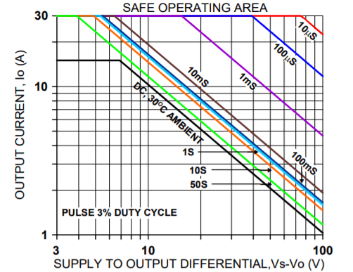
While the graph above adequately shows DC SOA and some pulse information it does not take into account ambient temperatures higher than 30°C, AC sine, phase or non-symmetric conditions that often appear in real-world applications. The PAD Power ™ spreadsheet takes all of these effects into account.
Step by Step Guide
Download and open the PAD Power spread sheet using the link provided above. At the bottom of the spreadsheet you will notice several page tabs. Click on “Readme” and study the introductory information on this page. We will expand upon the information in this article and add other details and tips as well.
Now click on the “Sine” page tab. You will notice a number of light-blue cells. These cells are for defining your application’s conditions for temperature, frequency and load. The spread sheet automatically recalculates results as you change operating conditions. You may find red pop-up information as you vary the input conditions. The information in red provides cautionary information or alerts you to dangerous conditions that need to be addressed. Don’t be concerned with the red warnings until all of your information is entered.
At cell E2 you may define the maximum junction temperature for the output transistors. A good rule of thumb is to set this number at 25°C less than the maximum junction temperature listed for the amplifier model used. Maximum junction temperature can be found in the specifications page for the amplifier model data sheet. Lower junction temperatures result in more reliable (longer life) application circuits and provide some margin in case some of the conditions specified later need to be estimated. In cell E2 type “150”.
Cell J2 defines the maximum ambient temperature expected. The amplifier needs clear open space around its heat sink to exhaust the hot air that is expelled by the amplifier’s cooling fan. This temperature may be higher than the temperature of the air going into the fan. Overall the “ambient” around the amplifier’s heat sink will be determined by the distance to various obstacles to free air flow around the amplifier, the power dissipation of the entire application circuit or system and how well the hot air is expelled from the system. At this stage of the analysis you may just have to estimate the temperature. At cell J2 type “30”.
Cell B4 defines the amplifier model. Click on this cell and you will find a pop-down menu with various amplifier models listed. For this example choose “PAD117”.
At cell E4 you will find another pop-down menu. Listed here are several common power amplifier application circuit configurations. For this simple example choose “Single Amp”. Whatever number is in cell G4 will be ignored when “Single Amp” is chosen.
Cells D6 and D7 define the power supply voltages. Note that amplifiers need some “head room”. That is to say, the power supply voltage needs to be higher than the expected output voltage peak. The amount of head room varies with the amplifier model and the peak output current. Refer to the product’s data sheet to find out what head room is needed for the expected peak output current and set the power supply accordingly. The specification of interest is “OUTPUT SWING”. Also consult the graph of typical output swing found in the “TYPICAL PERFORMANCE GRAPHS” pages of the data sheet. You also need to add the voltage drop in the connecting wires at the peak output current. It is usually not good practice to set the power supply voltage higher than needed because the excess voltage causes excess power dissipation in the amplifier which may limit the amplifier’s usefulness in the application and is wasteful of energy as well. In cell D6 enter “48” and in cell D7 enter “-48”. Needless to say the sum of these two numbers must be less than the maximum power supply voltage rating of the amplifier chosen. In this case the PAD117 is rated for 100V and the sum of the absolute values in cells D6 and D7 is 96V so this meets the requirement.
The next few light-blue cells define the signal expected at the load. At cell E10 select “Voltage” from the pop-down menu. This means that the intent of the application circuit is to control the voltage across the load. This is probably the most common application where some input voltage is amplified by some gain and the output voltage drives the load. At cell E11 type “90” and at cell I11 select “p-p” from the drop down menu. At cell H12 enter “0”. So far the output signal has been defined as a sine wave 90V p-p centered about 0 volts.
To further define the output signal enter at cell E13 “120” and at cell F13 enter “Hz” from the drop-down menu. At H13 enter “1” and at cell I13 enter “KHz” from the drop-down menu. At cell C15 click on “Continuous” from the drop-down menu. Altogether the output signal has been defined as a continuous 120 Hz to 1 kHz 90V p-p sine wave centered about 0V. Cells G15 and G16 will be ignored since “Continuous” was chosen at cell C15.
At cell E9 two types of analyses are offered: “use my input” and “find worst case”. Choose “find worst case”. When this option of chosen the input signal previously defined is interpreted as the maximum signal expected at the load and the temperatures calculated for junction and heat sink are the worst case expected as the signal across the load varies in amplitude, frequency and phase. More on this later.
The next few light-blue cells define the load conditions. For this example we will assume the PAD117 is driving a motor. The motor must be modeled as some inductance in series with some resistance. At cell B20 select “ohms=” from the drop-down menu and at cell C20 enter “10”. At cell B24 select “mH” from the drop-down menu and at cell C24 enter “3.3”. The motor is thus defined as 3.3mH of inductance in series with 10 ohms.
We will ignore lines 36 and greater for this example since these lines have to do with defining the load as some capacitance and resistance. Any red comments in this area can be ignored for this example.
At this point the amplifier model has been defined, its power supply voltages are set, and the output signal and load characteristics are defined. And we have chosen the “find worst case” analysis option.
Now it’s time to examine the results. To the right of the light-blue cells in the Load Definition section of the spread sheet you will find a number of cells in dark-blue. This area, ranging from cell D20 through G25, display the results of calculations made for the lower frequency entered in cell E13. In these cells you can find “Vrms”, the rms voltage across the load, “Arms”, the rms current in the load, and “Wrms”, the power the load is dissipating. Similar results for the higher frequency entered at cell H13 are displayed in the green cells H20 to K25.
More to the point of this exercise are the results displayed in dark-blue at cells F29 to F31. The results in these cells demonstrate one of the powerful features of PAD Power, namely, the “find worst case” analysis option chosen at cell E9. As the output signal amplitude and frequency vary the power dissipation in the amplifier varies as well due to the changing amplitude and phase relationship of the output current and voltage. Based on the input conditions given for maximum signal swing, power supply voltages and load conditions PAD Power calculates the worst case transistor junction temperatures and heat sink temperature (remember that the defined signal is interpreted as maximum when the “find worst case” analysis option is chosen). The results in these cells tell you if the amplifier will be overloaded anywhere in the operating range or not. The results listed for this example or well within the limits of the PAD117 and this application, as defined, will be quite reliable.
The PAD117 is a rail to rail operational amplifier. This means that it works equally well with the input pins biased to either supply rail or at any voltage in between. The output, even at high currents, also approaches the power supply voltages. The most common application utilizing this function is the single supply voltage amplifier where the +IN pin and the –Vs supply pin are grounded.
PAD Power can help with the analysis of a single power supply application as well. At cell D7 enter “0” and at cell D6 enter “48”. The application is now specified as a single supply of 50V (cell D6) and ground (0 volts) is specified for the negative supply voltage.
Since the output signal cannot be negative, because there is no negative supply voltage, the output signal must be re specified. The previous specification was an output signal of 48V p-p and a frequency range of 120 Hz to 1 kHz. Let’s leave that specification as is. But the center point of the output needs to be shifted from 0 volts to half of the p-p value. At cell H12 enter “24”. The output signal is now specified as 48V p-p centered about 24V.
The output signal now has an “offset” of 24V. An analysis consequence of the offset is that the spread sheet will no longer automatically find the worst case temperatures. At cell E9 the analysis option “use my input” must be chosen. The temperature calculation results shown in cells F29-F31 and cells J29-31 now reflect the defined signal but not necessarily the worst case temperatures as the signal amplitude and frequency vary. The temperatures displayed are largely determined by the DC offset and won’t vary much with the AC amplitude entered at cell E11. The user can manually adjust the signal and observe how the temperatures vary. Several signal amplitudes and offsets (if the offset varies) should be tried out and the resulting temperatures examined before the application can be determined as safe.
In this example you will note that the temperatures for the lower frequency (cells F29-31) are significantly different from the temperatures for the higher frequency (cells J29-31). This is due to the effect of phase difference between the output voltage and current at the high and low frequencies entered at cells E13 and H13.
It would appear that either of these applications with a frequency range of 120Hz to 1 kHz is good to go. Now that you are familiar with manipulating the input data for your application and you have seen how to interpret the results you should be ready for more complex analysis. Notice that there are more page tabs at the bottom the spread sheet. These sheets cover piecewise linear analysis for output signals of non-repetitive signals and also a page to help you with setting current limit for the various amplifier models using both standard and fold-over current limit. Explore these pages as you become more familiar with PAD Power.
AN-22
Single Supply Operation with Power Op Amps
Power Amp Design
Synopsis: The article outlines the problems and solutions for operating power op amps with a single high power supply voltage. Several application circuits are proposed that may help the user reduce system costs while maintaining high performance. Some familiarity with op amp circuits is assumed.
Although this article assumes some knowledge of operational amplifiers it may be beneficial for some readers to review a brief refresher on op amp theory. Other readers may feel free to skip to page 3.
Today’s operational amplifiers, whether constructed from discrete components or a monolithic chip, approach many of the characteristics of the ideal differential gain block of Figure A. The ideal differential gain block is characterized by infinite gain and bandwidth, infinite input impedance, zero output impedance and zero differential input error. These characteristics imply that the overall performance of an application circuit is determined by the external components connected to the op amp.
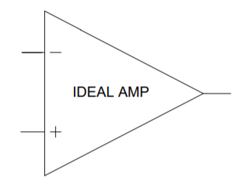
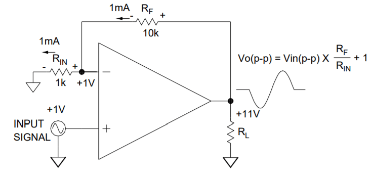
It is easier to analyze any op amp circuit if you keep the ideal characteristics in mind and also remember that the action of any op amp circuit is to swing the output to such an amplitude and polarity that the two inputs (+ and -, noninverting and inverting respectively) are at the same voltage. The op amp accomplishes this through feedback, i.e. the external components tied between the inputs and the output of the op amp. The inverting input is so named because a positive going signal (for example) at this input forces the output of the op amp to be negative going. The non-inverting input does the opposite; a positive going input signal on the non-inverting input forces the output to also be positive going. The circuit in Figure B, for example, can be easily analyzed using these principles.
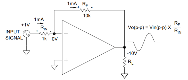
Note that the non-inverting input of the amplifier is grounded (zero volts). Since the ideal amplifier has zero differential error the inverting input must also be at zero volts (virtual ground). If the input voltage is +1V then 1mA flows into the inverting node (-). Remember that for the ideal amplifier no current flows into the inputs (infinite input impedance). The entire 1mA therefore must flow into RF (10k). The resulting voltage at the output of the amplifier must be -10V (1mA X 10k). This is the basic inverting amplifier configuration.
A similar analysis can be performed with an input signal tied to the noninverting input of the op amp. In Figure C, +1V is tied to the + input of the op amp. As before, since there is no differential error between the inputs of the op amp, the inverting input must also be at +1V. The output of the amplifier swings in a direction (polarity) and amplitude to make this so. The +1V causes 1mA to flow into ground from the inverting node. The same 1mA therefore flows through RF (10k) developing 10V in doing so. Since one end of RF is tied to +1V the other end must be at +11V and this accounts for the signal gain of +11 as opposed to the inverting amplifier signal gain in Figure B of -10 using the same values for RIN and RF. This is the basic non-inverting amplifier configuration.
These simple concepts will help in analyzing any op amp circuit.
If you skipped the op amp primer you can pick up the discussion here:
From the very beginning operational amplifiers have been powered by positive and negative power supplies ─ ±15 Volts, for example, is very common. There are good reasons for this: the dual supplies overcome possible biasing problems with the internal design of the op amp and, from an external point of view, it allows the output of the amplifier to reach zero volts. The dual power supplies also allow for reversing of a grounded motor load, for example. The dual supply approach works very well but there is a cost impact as well.
In the last several years a plethora of small signal op amps have reached the market that can operate on a single power supply. Some of these designs are “rail to rail”, or RRIO, standing for rail to rail input and rail to rail output; i.e. both the input and output voltages can swing to the power supply voltages. In the case of the output specification “rail to rail” is really only an approximation. As the op amp output transistors sink or source current some voltage drop necessarily occurs. At the inputs of the op amp, however, “rail to rail” is actually achievable.
In the case of power op amps the situation is a little different. As opposed to the milliamp output of its small signal cousins the power op amp can provide an output of a few amps to several tens of amps depending on the model. Power op amps usually do not operate RRIO although a few IC power op amp models on the market do have an input common mode range that includes the negative supply voltage (see discussion below).
Thus far Power Amp Design is unique in this way. To date Power Amp Design has two RRIO models, the PAD117 and the PAD127. Like their small signal brethren these two models cannot supply output current without dropping some voltage, but the PAD117, for example, can supply 15 amps with only a 1.5 volt drop from the power supply voltage. The PAD127 can do likewise with a 30 amp output.
The major reasons for operating a power op amp with a single supply voltage are system cost and/or weight. While providing ±15 volts for a small signal op amp may not entail much cost a second power supply that can provide 10 or 20 amps at 50 or 100 volts would be of considerable expense and weight.
Two important op amp specifications need to be examined when considering a power op amp for a single supply application: input common mode range and output swing under load.
The input common mode range specifies how closely the inputs of the op amp can approach the power supply rails and still have the op amp operate correctly. In every op amp circuit the two inputs are maintained at virtually the same voltage owing to feedback in the external circuit. When the input voltage is pushed beyond the common mode range of the amplifier the internal biasing requirements of the op amp are no longer met and the output of the amplifier cannot swing to the correct output voltage. Often the common mode range is not symmetric, i.e. the inputs may be allowed to swing within 2 volts of the negative power supply voltage, but only within 5 volts of the positive power supply voltage. Some amplifiers allow the inputs to go all the way to the negative power supply voltage and these designs are often referred to as having a “common mode range that includes ground”. Power Amp Design’s model PAD117 is such an amplifier.
The output swing capability specification of the power op amp is also important. At high output current the output voltage of an ordinary power op amp may drop as much as 7 volts from the power supply voltage. If, for example, a single supply application is powered by +48 volt power supply the output swing may be limited to 34 volts total owing to the 7 volt drop from each supply rail (+48V and ground ─ the negative supply). The voltage drop from each power supply rail limits the output swing and reduces the efficiency of the circuit. The wasted power ends up as a higher amplifier operating temperature.
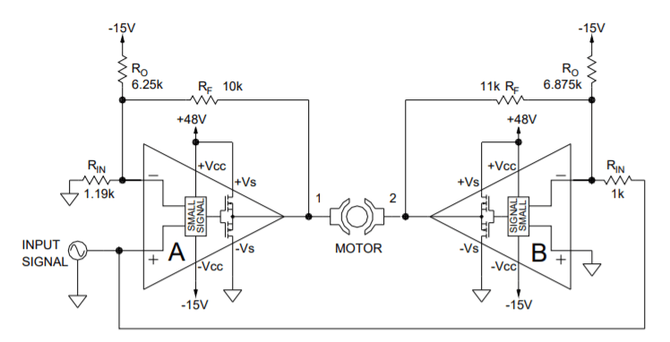
In the most usual single supply configuration (Figure 1) a power op amp is powered by a positive power supply (+VS) and the negative power supply connection (-VS) is tied to ground (common). A common design challenge with this configuration is that the non-inverting input must be floated to some positive voltage to meet the common mode requirement of the op amp. A few power op amps on the market have a common mode range that includes the negative supply voltage, but this is rare. From a biasing point of view the output stage doesn’t care if only one polarity of power supply voltage is available, but the input stage does care unless especially designed so that its common mode range includes the negative supply voltage.
At this point a distinction needs to be addressed. Traditionally, op amps have only two power supply connections, +VS and –VS. Most of the op amps on the market today are powered in this way. Consequently “single supply” has come to mean that the entire op amp must operate from these two power inputs, one of which is grounded for single supply operation. But, for power op amps, all that is really needed is for the output stage of the op amp to operate from a single supply voltage since eliminating one high power supply is where the cost savings come from. The small signal stages of the op amp are not required to operate from a single supply voltage even if the amplifier’s output stage is.
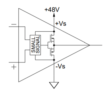
Power Amp Design models have significant advantages when applied to single supply applications when compared to most monolithic or hybrid power op amps. Power Amp Design models usually operate from four power supply voltages, +Vcc, -Vcc, which are connected to the amplifier’s small signal stages, and +Vs and -Vs which are connected to the amplifier’s output stage. In many or most applications +Vcc and +Vs are tied together and, likewise, -Vcc and Vs are connected. But these connections are not required. (The four power supply connections are not provided in the RRIO models PAD117 and PAD127 as this feature is unnecessary for RRIO designs.)
Let’s look at an application (Figure 2) where bipolar system power supplies are available to power the small signal stages of the amplifier but the output stage is powered from a single high power supply.
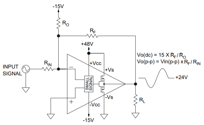
The circuit in Figure 2 takes advantage of the four power supply voltages available in Power Amp Design op amp models. The figure shows the power supply connections to the small signal (input) stages of the op amp and also the power connections to the output stage MOSFET transistors. While the positive power supply connections are connected together (+VCC and +VS) the negative power supply connections (-VCC and -VS) are not. Instead, -VCC is connected to the system -15V power supply and the output stage -VS is tied to ground. Connecting the system -15V power supply to the small signal stage of the power op amp is usually not a burden since the small signal stages of the op amp typically draw only a few milliamps.
The alternate connection for -VCC provides two benefits. One benefit is that the common mode input voltage range specification is met. The non-inverting input is grounded and thus is 15V from the negative supply voltage (-VCC). Some op amp output stage designs (PAD128, for example) benefit from a second and less obvious advantage: the drive to the output stage transistor connected to -VS has an additional 15V of drive voltage available. Thus the output transistor can drive the output voltage much closer to ground than would otherwise be possible.
Another feature of the circuit in Figure 2 utilizes the -15V to generate a +24V offset at the output of the amplifier. Thus any AC input signal will swing plus and minus about the +24VDC level at the output of the amplifier. If the -15V wanders with load or temperature the output of the amplifier will wander as well. It is therefore best that the -15V be either regulated and temperature stable or that it be regulated to some other lower voltage that is stable.
The amplifier has some offset voltage that drifts over temperature. For power op amps typical offset voltages range from 1 to 5 mV and drifts up to 50µV/°C. The amplifier’s offset voltage is magnified at the output by the DC gain of the amplifier as set by the feedback network. Any offset externally set by the circuit should be at least as stable as the offset of the amplifier.
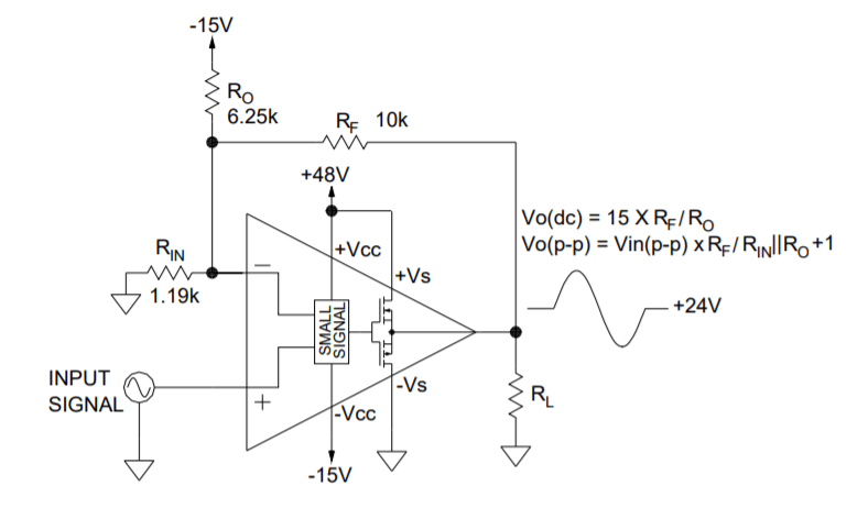
Figure 3 below shows another circuit similar to the inverting circuit of Figure 2, but non-inverting. Mathematically this circuit is a little more complicated since RO and RIN appear in parallel (the || symbol in the equation) in calculating the gain of the circuit. Example resistor values are given to illustrate a signal gain of 11 while the output is offset to a DC value of +24V.
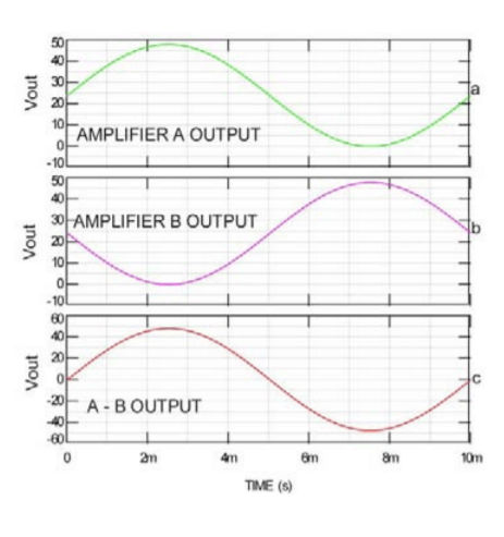
In Figure 4 below, the ideas of Figure 2 and Figure 3 are combined into a bridge circuit to drive a brush motor. While Amplifier A’s output is going positive (Figure 5a) Amplifier B’s output is going negative (Figure 5b). The result is that up to 96V p-p (Figure 5c) is available to drive the motor from a single +48V power supply (neglecting voltage drops across the output stage of each amplifier). The signal gain of each amplifier is 11 and the total signal gain that appears across the motor is 22 for the values shown. Another way to interpret the output of the bridge circuit is that the motor can be driven to 100 % RPM in either direction depending of the polarity of the input voltage.
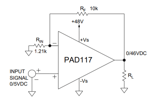
In another system there may be no negative small signal power supply available. In the simplest case a unipolar input signal results in a unipolar output voltage from the amplifier. In Figure 6, a 0/5V signal results in a 0/46V output voltage from a PAD117 RRIO power op amp from Power Amp Design. With no load current the PAD117 output can reach zero volts. The input is also rail to rail capable so an input voltage of zero volts does not violate the common mode range of the amplifier. This is an application where the RRIO power op amp is very helpful since few external components are needed to make the amplifier work properly.
Still another circuit, both more versatile and more complicated, is shown in Figure 7, below. In this circuit a charge pump circuit converts the high voltage positive supply voltage into a negative low voltage reference voltage suitable for establishing a +24 volt offset at the output of the power amplifier.
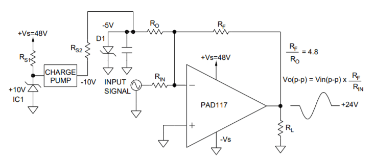
The amplifier in Figure 7 is a PAD117 from Power Amp Design and is a RRIO design. The non-inverting input can be grounded and not violate the input common mode range of the amplifier. The gain of the amplifier stage is easily varied as is the output offset voltage by adjusting RF, RIN and RO. For maximum output offset stability D1 is a reference integrated circuit that acts like a zener diode, a National LM4040DIM3-5.0, for example. The charge pump voltage inverter circuit is constructed using a Microchip TC7660 integrated circuit. The TC7660 requires two external capacitors (not shown) to make the voltage conversion.
Summary
Traditionally op amps have only two power terminals. Since one power terminal is grounded for single supply applications some sort of input biasing scheme must be used to satisfy the input common mode voltage requirements of the op amp. While it is possible to overcome this problem with an input stage design that has a common mode voltage range that includes the negative supply voltage this type of design is rare for power op amps. Overall it is more beneficial for a power op amp to have four power terminals where the small signal stages of the power op amp and the output stage are powered separately so that the input stages of the op amp can take advantage of the low voltage power supplies that may already be available in the system. It is also more beneficial to use power op amps that are of a RRIO design since this design is easier to bias in single supply applications and provides a more efficient use of the power supply voltages available since the output of the RRIO design swings much closer to the supply voltages than any other power op amp designs. To date Power Amp Design is the only manufacturer with RRIO power op amp designs available.
AN-24
Eliminating Circuit Noise from Cooling Fans
Power Amp Design
Synopsis: The article covers the electrical noise considerations for connecting the cooling fan of Power Amp Design power op amps to the signal circuits.
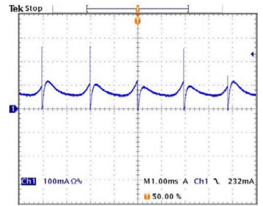
Most power op amps currently produced by Power Amp Design rely on an integrated heat sink and fan to provide adequate cooling for the amplifier. The standard fan supplied with the amplifiers is a 12V brushless DC motor fan. Like all switching circuits, the brushless fan motor commutation generates electrical noise. If care is not taken in how the fan is connected to the amplifier circuit some of that electrical noise may appear at the output of the amplifier.
In Figure 1, below, the current in the return (minus) lead of the fan motor is displayed. The current spikes are approximately 250mA in amplitude. This is the source of the voltage spikes that can be observed in the output waveform shown in Figure 2.
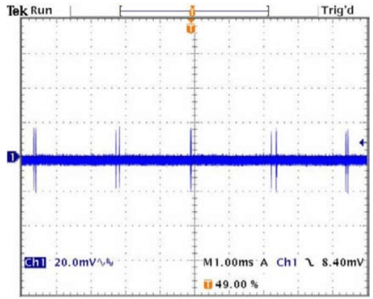
In Figure 2, the switching noise of the fan motor can be seen at the output of the amplifier. The noise is approximately 40mVp-p with the amplifier in a gain of 20. The amplitude of the noise will vary with the gain of the amplifier. The actual noise is often related to the input as RTI (referred to input). In this case a noise of 2mVp-p at the input will produce the output seen in Figure 2. The amplitude at the output of the amplifier will also depend on the rise and fall times of the current spikes.
Experiments have shown that this noise is injected into the amplifier’s common connection (ground) caused by the current spikes in the fan motor as shown in Figure 1. In many applications the noise is not objectionable, but it is easy to eliminate it altogether. The 12V power supply for the fan circuit is often isolated. Leaving this power supply isolated its minus output not connected to the amplifier’s common) will eliminate the noise and no components are required. Another method is to connect a 47-100µF electrolytic capacitor on the circuit board directly at the physical point where the leads from the fan connect to the circuit. Twisting the fan lead wires into a twisted pair, while neat, does not reduce the noise, but it is good practice to cut the fan lead wires to the shortest practical length before attaching to the circuit board.
Circuit layout is also important. The waveforms in Figure 1 and Figure 2 were taken from an evaluation kit PCB with a ground plane connecting all the common connections for the circuit. Nevertheless, the fan motor current spikes were able affect the input to the amplifier. It is important that the return current from the fan motor not be mixed with the signal path common. A large ground plane and/or a single point ground connecting all the commons of the circuit will help reduce or eliminate any switching noise at the output of the amplifier.
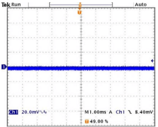
Figure 3 shows the result at the output of the amplifier of connecting a 47µF electrolytic capacitor directly at the point where the fan leads connect to the evaluation circuit board. The remaining noise is due to pickup of other noise sources. By a combination of careful circuit layout and adequate bypassing of the fan power supply connection all of the switching noise can be eliminated from the output of the amplifier.
AN-26
About Power Ratings
Power Amp Design
Synopsis: A brief discussion of the meaning of power ratings as they relate to power operational amplifiers.
When we want to purchase a home stereo amplifier we might consider the power rating of the amplifier, say a 100 watt amplifier model vs. a 200 watt model. What does the power rating mean? Does the power rating mean something different for a power op amp?
In the audio amplifier market there are many definitions for the power ratings of an amplifier but they all relate to the power that can be delivered to the load (speakers) and the rating always relates to sine wave signals to the load. DC to the load is not considered (we can’t hear DC) and even avoided in the amplifier design since DC to a speaker can damage the speaker voice coil.
With home audio amplifiers there is also no discussion, or rating, of the power dissipation capability of the amplifier or often even a rating for the temperature extremes over which the amplifier can operate safely. It is assumed that the amplifier is going to operate in the home and that the ambient temperature is not going to vary much. And since the amplifier is purchased as a whole unit the user does not need to consider the power dissipation capability of the amplifier ─ that was the job of the amplifier designer.
But with applications in the industrial world we do need to consider ambient temperature, DC operation and other factors safely ignored in home amplifiers. Although the power operational amplifier (power op amp) can be used as an audio amplifier the language for power ratings of industrial power op amps is quite different. For one thing, the hyperbole of consumer marketing advertisements for home stereo amplifiers is usually avoided since engineers are probably going to see through the hype and are looking for solid technical information that insures their application circuit is going to be reliable.
A power op amp is considered a component since the op amp needs power supplies, other components and a printed circuit board to connect all the pieces together to produce a finished amplifier. As such, the designer of the application circuit using a power op amp must consider the ambient environment, both the DC and AC power dissipation capability of the power op amp, and the required power needed to drive the load.
Integrated circuit or hybrid component power op amps are usually rated, not for their power output capability, but for their DC power dissipation capability, with the amplifier case (the area connected to the heat sink) at 25°C and the junction of the power transistors in the output stage of the amplifier at their maximum rated junction temperature (usually 150°C or 175°C). This is just a reference point so that various products can be compared in that regard and doesn’t reflect an operating condition that is usually achievable in a real-world application.
To calculate the actual power dissipation capability of a power op amp the application designer needs to know the thermal resistance of the amplifier itself (junction to case), the power dissipation expected in the application, the thermal resistance of the interface material between the amplifier and the heat sink (thermal grease), the thermal resistance of the heat sink and the ambient temperature expected for the application.
Consequently, a component power op amp rated for 125W might, in a real-world application, only be capable of 50W of power dissipation or even less. This is a common result with commercially available heat sinks, even with those heat sinks made available by the manufacturer for their products.
Power Amp Design power op amp products are rated differently since our amplifiers are supplied with integral heat sinks and fan cooling. Our amplifiers are still component power op amps but most of the derating factors have been eliminated for the user. When we rate an amplifier for 100W we mean the amplifier can dissipate 100W DC with 30OC air at the fan inlet. And since there are no other factors to derate the amplifier dissipation capability, the 100W dissipation capability is readily achievable. In short, our dissipation rating of 100W means 100W DC in real-world applications and the designer doesn’t need to apply any derating factors other than the ambient air temperature expected.
Dissipation capability for AC signals is usually significantly higher than for DC signals. For AC signals the output transistors (usually two, an N type and a P type) are able to share the load and thus the apparent thermal resistance of the amplifier is lower. But Power Amp Design doesn’t use AC thermal resistance to rate a power dissipation rating capability. We use the AC thermal resistance to rate output power capability with AC signals. By output power capability we mean the maximum continuous RMS power delivered into a resistive load when the output signal swings to its maximum peak to peak value with the maximum power supply voltages applied. This is a somewhat ideal condition but one that can do useful work in a real-world application. Some manufacturers refer to the power delivered to the load with the amplifier locked up to one supply rail. This condition does deliver the maximum power to the load, but this is not a useful condition in most real-world applications.
The real measure of a power op amp is not the power it can deliver to the load but the power dissipation the amplifier must withstand while delivering that power. It’s usually not easy to calculate the maximum power dissipation an amplifier must tolerate in an application circuit, especially with reactive loads. To solve this problem Power Amp Design has developed a custom Excel based design spreadsheet called PAD Power™ that can easily calculate power dissipation, junction temperatures and heat sink temperatures given all the circuit parameters for load, signal and power supply voltages for each of the power op amp models available. PAD Power is available free and can be downloaded from the website.
AN-28
Power Op Amp Specifications Discussion
Power Amp Design
Synopsis: The meaning of the performance specifications for power op amps is discussed with tips and insights.
Each power op amp datasheet will have a specifications page listing the model’s performance specifications. For Power Amp Design op amp models the specifications are usually grouped by: INPUT, GAIN, OUTPUT, POWER SUPPLY, THERMAL and FAN. Each of the specifications will be discussed in turn as they appear in most op amp datasheets manufactured by Power Amp Design. Some familiarity with op amp theory is assumed, but a review of the specification discussions below may serve as a refresher course. For another op amp theory refresher you may refer to the first three pages of AN-22 Single Supply Operation with Power Op Amps.
INPUT
OFFSET VOLTAGE: In an ideal op amp the two inputs, via feedback, will assume the same voltage. The two inputs are the input nodes to a differential amplifier whose purpose is to amplify the difference of the two input voltages. One input is termed the inverting input (-) and the other the noninverting input (+). The feedback of the amplifier from output to input is arranged so that the output voltage swings the proper amplitude and polarity so that the difference in voltage between the inputs is cancelled. But in practical op amps the input differential amplifier is not perfect and so some error voltage will exist. The offset voltage is this error, usually expressed in mV. Once the output of the amplifier has stabilized, a DC voltage can be measured between the two inputs and this is the offset voltage. Offset voltages between 1 and 5 mV are commonly specified and are assumed to be of either polarity. The voltage at the output of the amplifier with an input voltage of zero volts will be the dc gain of the amplifier times the offset voltage. For example, if the offset voltage is 1mV and the dc gain of the amplifier is 10 then 10mV will be measured at the output of the amplifier.
OFFSET VOLTAGE vs. temperature: The DC error of the input differential amplifier as discussed in the OFFSET VOLTAGE section above also has a temperature effect. The offset voltage can drift over temperature anywhere from 1 to 50 micro-volts per degree Centigrade (µV/°C) of either polarity. Although the drift can be linear with temperature it usually is not. Either an “S” curve or “U” curve is usually noted as the offset voltage vs. temperature is plotted. However, the intent of the specification is to show that the change in offset between any two temperatures over the specified range will not change by more than the maximum specified drift per °C.
OFFSET VOLTAGE vs. supply: Yet another error specification related to offset voltage. The offset voltage as discussed above also changes with power supply changes. Op amps are designed to operate properly with a range of power supply voltages, both positive and negative. As the power supply voltages change the offset voltage will also change by some amount, usually expressed as micro-volts per volt of power supply change (µV/V). The offset change is usually different when the positive power supply voltage changes as when the negative power supply changes, but the specification takes the worst of the two changes into account.
BIAS CURRENT, initial: This specification also refers to the input differential amplifier and is a measure of the current required to operate the input differential pair of transistors. The bias current is often measured in pico-amps (pA). Power Amp Design power op amps use JFET transistors as the input differential pair and the bias current is exceedingly low. Although usually specified as 100pA maximum the bias current is usually much lower. Leakage to other circuit components is usually more than the actual bias current of the JFET transistors, but the bias current specified is the current that might be measured going into or out of the input pins, either positive or negative for each input pin.
BIAS CURRENT vs. supply: The bias current may change with the power supply voltage, usually specified as pico-amps of bias current change per volt of power supply voltage change (pA/V). This specification cites the maximum the bias current is likely to change as the power supply voltage changes.
OFFSET CURRENT, initial: The bias current to each input pin may not be the same value or polarity. The offset current is the difference between the two bias currents.
INPUT RESISTANCE, DC: The fact that some current flows into or out of the input pins means that the equivalent resistance of the inputs to the power op amp is not infinite as would be the case for an ideal amplifier. The equivalent resistance is specified in gig-ohms (GΩ). The JFET transistors connected to the inputs of the amplifier look like reversed biased diodes and have very high equivalent resistance, usually specified at 100 GΩ for Power Amp Design models.
INPUT CAPACITANCE: The signal inputs to the power op amp also have an equivalent capacitance specified in pico-farads (pF). The input capacitance for Power Amp Design models is usually specified as 4 pF. While in an ideal op amp the input and feedback resistances could be any value without an effect on the circuit, in a real world op amp the input capacitance forms a pole with the input and feedback gain setting resistors and therefore has an effect on the frequency response of the op amp circuit.
COMMON MODE VOLTAGE RANGE: This parameter specifies how closely the input voltages can approach the supply voltages in normal operation. Often there are two separate specifications, one specifying a voltage from the positive supply voltage and the other specifying a voltage from the negative supply voltage. For example, model PAD113 is specified as having a common mode voltage range of +Vcc-15V and –Vcc+7V. This means that the input pins in normal operation cannot be any closer than 15V from the positive supply voltage or any closer than 7V from the negative supply voltage. The common mode voltage range most often becomes a concern when one of the power supply voltages is minimum. For example, considering again the PAD113, the common mode voltage range to the negative supply voltage is –Vcc+7V. If the + input is grounded (as it often is for an inverting amplifier application) the negative power supply voltage could not be less than -7V (for example, -6V would not be allowed in this case). RRIO amplifier designs (rail to rail input and rail to rail output) like the PAD117, however, allow the input voltages to be the same as the power supply voltages. For a RRIO power op amp design the +input could be grounded and the negative power supply pin could also be grounded (single supply operation) and satisfy the common mode voltage range parameter.
COMMON MODE REJECTION, DC: As the input voltages move from near the negative power supply voltage to near the positive power supply voltage the offset voltage of the amplifier will change due to changing voltage drops across the internal components. How much the amplifier rejects any offset voltage changes is expressed in dB down from the original offset voltage value and is RTI (referred to input). Previously, under the offset voltage explanation, it was mentioned that the offset voltage is multiplied by the DC gain of the amplifier circuit, so that a 1mV offset between the inputs will result in a 10mV output for an amplifier circuit in a gain of 10. Therefore, when the gain of the amplifier circuit is known to be 10 and 10mV of output is observed the offset RTI (referred to input) is only 1mV (assumes a zero input voltage to the amplifier circuit). Although the gain of the circuit may change the output value, the RTI offset voltage does not change. Another specification that is related to Common Mode Rejection, DC, is Power Supply Rejection, DC. Although expressed differently as micro-volts per volt (µV/V), power supply rejection is virtually identical to common mode rejection. From the viewpoint of the amplifier’s inputs there is no difference between moving the inputs relative to the power supply voltages and moving the power supply voltages relative to the inputs.
NOISE: Although an amplifier’s noise can be expressed in several ways we specify the total noise within a brick-wall bandwidth of 100 kHz with a source impedance of 1kΩ. Since the source resistance itself is a noise source its noise will also be measured at the output of the amplifier. But in the real world some input resistance will be needed to set the gain of the amplifier and 1kΩ was chosen as a reasonable value for actual circuits.
GAIN
OPEN LOOP: Open loop gain is often abbreviated as Aol. It is the maximum gain that the amplifier produces at a stated frequency, often DC. The open loop gain is so stated because it is specified as the gain with no feedback elements that would set the overall amplifier circuit gain (closed loop gain). A graph of the open loop gain of the amplifier is given with a Bode plot which is provided in the data sheet in the typical performance graphs for each model. The Bode plot is important because it can graphically show the accuracy the amplifier can attain at any frequency within its range by plotting the closed loop gain (the gain determined by the external feedback elements) of the amplifier circuit on the Bode graph and taking the difference between the open loop curve and the closed loop curve. For example, say that at DC an amplifier has an open loop gain of 100dB. The amplifier circuit is in a closed loop gain of 10 (20dB). The difference between the open loop gain and the closed loop gain at DC is 80dB. Expressed linearly 80dB equals 10,000. So the gain accuracy you might expect from the amplifier due to open loop gain limitations would be 1 part in 10,000 or 0.01%. As the closed loop gain of the amplifier circuit goes up the corresponding gain accuracy goes down. In the example above let’s say the DC gain of the amplifier circuit goes up to 100 from the 10 previously considered. The difference between the open loop curve for the amplifier and the DC gain curve is now only 60dB or 1000 and the corresponding gain accuracy we could expect drops to 1 part in 1000 or 0.1%. So, the higher the open loop gain at any frequency the better the expected gain accuracy at that frequency.
GAIN BANDWIDTH PRODUCT: is usually expressed in units of MHz (megahertz) at some specified frequency, often at 1Mhz. When the bode plot of the amplifier is examined to determine the gain at the specified frequency the gain bandwidth product is simply that gain multiplied by the stated frequency. For example, if the bode plot of the amplifier crosses zero dB (gain of 1) at 1 MHz then the gain bandwidth product of that amplifier is 1Mhz at 1Mhz. Another amplifier may have a gain of 20dB (gain of 10) at a frequency of 1MHz and therefore that amplifier would have a gain bandwidth 10MHz if the specified frequency is also 1 MHz.
PHASE MARGIN: For a feedback amplifier (such as an op amp) the worst case for a stable circuit occurs when the feedback ratio is 100% (unity gain follower). Amplifiers are usually designed to minimize phase shift so that there is at least 60° of phase margin; that is to say the op amp’s internal circuitry shifts the phase of the input signal by no more than 120°. If the op amp is externally wired as unity gain follower and the phase shift were 180° then that circuit would be sure to oscillate. A phase shift of 45° is usually considered the minimum phase margin to insure stability. However, the amplifier’s load also causes phase shift as it interacts with the closed loop output impedance of the amplifier and this is why it is desirable that the amplifier have as much phase margin as practical. Power op amps most commonly drive rather nasty loads when considering stability. It is therefore desirable to configure the gain circuit of the power op amp to have some gain greater than unity. As the gain increases the feedback percentage drops and makes an unstable circuit less likely. Power op amp loads are often not well defined, especially across a frequency band. A gain larger than unity helps insure a stable circuit. A gain of 10 or more is often recommended, especially for loads that are highly reactive (more common than not).
OUTPUT
VOLTAGE SWING: Specifies how closely the output of the amplifier can approach the power supply voltage feeding the amplifier when supplying a specified output current. The voltage swing depends on load current and is usually different for positive and negative output current. Even with no output load current most amplifiers are unable to drive the output voltage all the way the power supply voltage owing to the amplifier’s internal bias considerations. However, so called RRIO (rail to rail input, rail to rail output) amplifiers come closest to achieving this.
CURRENT, continuous DC: usually the minimum output current capability of the amplifier. Power op amps usually can provide much more output current than specified as a minimum, especially with short term pulses, but the amplifier’s limitation is usually the power dissipation while providing that current and it’s the power dissipation capability that often sets the output current specification.
SLEW RATE: the maximum rate of change of voltage at the output of the amplifier between the 10% and 90% of the maximum output peak to peak voltage, specified as V/µS. A gain and a compensation capacitor value are also usually specified. As the compensation capacitor value decreases the slew rate increases. It is common for power op amps to have slew rates greater than that necessary to support their small signal bandwidths. This is easy to see via the square wave response of the amplifier where distinct rounding of an output square wave may be evident. However, common applications for power op amps involve driving sine wave outputs into loads and the higher slew rate translates into higher power bandwidths, a distinct advantage.
POWER SUPPLY
VOLTAGE: the power supply operating minimum and maximum voltages are given as a plus and minus value (±) since power op amps are usually operated from two power supply voltages. The amplifier can operate with supply voltages anywhere between these values. In addition the amplifier can operate with a single supply as long as common mode restrictions are met (see above under COMMON MODE VOLTAGE RANGE). If an amplifier’s power supply voltage is rated from ±8V to ±50V it can also operate from a minimum single supply of 16V to a maximum of 100V either plus or minus and the other supply pin at zero (again, assuming common mode voltage range restrictions are met). The power supply voltages may also be unbalanced. For the amplifier specification of ±8V to ±50V power supply voltages of -10V and +90V also meet the power supply voltage specification.
CURRENT, quiescent: the various stages of the amplifier require some current to operate correctly and the sum of these currents is called quiescent current. This current varies over temperature and also with power supply voltage and graphs of these variations are plotted and presented in the typical performance graphs section of the datasheet. For power op amps most of the variation in quiescent current over temperature results from drift in the output stage bias current. In addition it is common for the quiescent current versus supply voltage variation to be more sensitive to one supply voltage variation than the other, but the worst of the two is specified.
THERMAL
RESISTANCE, AC, junction to air: measured in °C per watt (°C/W) of power dissipated in the amplifier. Anytime an amplifier dissipates power the temperature of the amplifier’s output transistors will rise. The lower the thermal resistance of the heat path of output transistors the lower the temperature rise. Lower operating temperature is essential to high reliability. If the temperature rises too much the output transistors will be destroyed. In the case of AC thermal resistance each of the two output transistors share the load─ each of the two output transistors conducting current on alternate half cycles. Since the temperature of each output transistor affects the temperature of the other transistor the AC thermal resistance is not one half of the DC thermal resistance. As the frequency rises from DC, the AC thermal resistance drops until it reaches its minimum point at about 60Hz.
RESISTANCE, DC, junction to air: similar to AC thermal resistance as above, but considers the thermal path of only one of the two output transistors since only one transistor at a time can conduct current.
TEMPERATURE RANGE, ambient air: the ambient air temperature is the temperature of the air immediately surrounding the amplifier’s environment. The environment temperature is affected by the heat generated by the amplifier as it dissipates power. It is therefore important that some means is employed to remove the air with elevated temperature. The fan intake must have a continual source of fresh cool air to maintain the amplifier within its
operating temperature range. The ambient air temperature specification is limited by the operating specifications of the fan. The amplifier itself is capable of operating over a wider temperature range. Due to the thermal drop across the heat sink, the temperature of the amplifier’s substrate is higher than the temperature of the fan. So while the fan is limited to a temperature range of -40 to +70 °C, the amplifier substrate can operate over a temperature range of -40 to +105 °C.
TEMPERATURE, shutdown, substrate: the amplifier is equipped with a precision sensor that monitors the temperature of the amplifier’s substrate. When the substrate temperature exceeds 110 °C the sensor circuit activates a
shutdown signal that turns off the output stage of the amplifier. The substrate temperature must fall by 10 °C before the amplifier’s output stage is enabled once again. The sensor measures average substrate temperature and so it is
possible that an overload of the output transistors might occur so quickly that the output transistors may be destroyed before substrate has had time to heat up to the point that shutdown will occur. However, the sensor will protect the amplifier against slow thermal overloads and fan circuit failures.
FAN
OPERATING VOLTAGE: the nominal operating voltage for the fan that produces the thermal resistance specifications as above. The nominal voltage is 12V but the entire range of the fan is 7-17V. Running the fan at a voltage above the nominal does not improve the thermal rating of the amplifier.
OPERATING CURRENT: the current required to operate the fan at the nominal voltage. The fan is operated by a brushless motor controller inside the fan housing. The controller is a switching circuit and can produce voltage noise due to the current pulses from the switching circuits. It is recommended that a 47µF electrolytic capacitor be used to filter the current pulses. The bypass capacitor should be placed directly at the point where the wires leading to the fan connect to the 12V power supply for the fan.
AIR FLOW: this is the rated air volume for the fan used before it is attached to the heat sink. Due to the resistance that the heat sink fins provide the air flow will drop when the fan is mated to the heat sink. This is a useful specification to have should the fan ever need to be replaced.
RPM: this is the rated revolutions per minute of the fan used before it is attached to the heat sink. Due to the resistance that the heat sink fins provide the RPM will drop when the fan is mated to the heat sink. Another useful specification to know should the fan ever need to be replaced.
NOISE: this is the audible noise the fan generates. As the RPM drops the noise drops as well.
L10, life expectancy, 50 °C: L10 refers to the time it takes for 10% of a population of fans to fail. Lower ambient temperature increases fan life. This is a different specification than mean time to failure. Mean time to failure requires that 50% of a population of fans fail. While the L10 failure time is 45k hours for the fans we use an equivalent mean time to failure is 200k hours.
Although some amplifiers may have additional specifications the above discussion covers all of the common specifications you will find in our power op amp datasheets. Our application engineers are always available to answer questions about our products and are happy to assist you with your application circuit development. In addition, each amplifier product has a companion evaluation kit available to help you rapidly develop your circuit without having to research supporting components and construct a circuit board.
AN-32
Using Evaluation Kits to Implement Parallel Operation
Power Amp Design
Synopsis: How to use two or more evaluation kits to connect power op amps for parallel operation.
An increasingly popular application calls for paralleling power op amps either to increase the available output current or sharing the power dissipation among two or more amplifiers. In this article we will show the top level schematic for connecting power op amps in parallel and also how to use two or more evaluation kits to implement parallel operation. For examples, we will refer to the EVAL118 evaluation kit for the PAD118 High Power Operational Amplifier since this is a common amplifier model used for parallel operation.
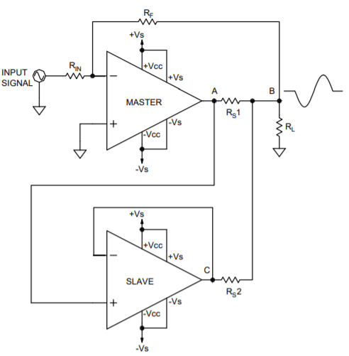
INVERTING PARALLEL OPERATION
Figure 1 illustrates the top level schematic connections for two amplifiers in parallel. The circuit is inverting. The output of master amplifier (node A) is also the input signal to the slave amplifier connected as a unity gain follower. Notice that the feedback to gain setting resistor RF is connected to the output of the combined circuit (node B) whereas the feedback for the slave amplifier (node C) is connected directly to the output of the slave. Between nodes A and B and also nodes C and B you will notice balance resistors Rs1 and Rs2. These resistors help insure that the amplifiers share the load current for the inevitable case where the slave has some offset. The master amplifier can, of course, drive more than one slave. The slave connections can be repeated for additional slave amplifiers.
When the EVAL118 is not used for parallel operation Rs1 (Rs on the circuit board) is intended as a current sense resistor used in conjunction with the PAD121 Current Limit Accessory module. But for this parallel application the current sense resistor will double as a balance resistor. Later we will show how these balance resistors can also be used to set the current limit trip point. See the datasheet for the PAD121 for complete details on its operation.
In the case of the PAD118 power op amp, a current limit function is not built-in but relies on the PAD121 to perform that function. The EVAL118 supports the PAD121 with a plug-in slot. The PAD121 can be programmed to select one of several modes of current limit operation. Basic operation of the PAD121 is pre-wired on the EVAL118 circuit board with jumpers that connect its inputs to Rs1 (Rs on the circuit board) as shown in the above schematics. When the output current of the amplifier reaches the set point (±150mV across the current sense resistor Rs) the PAD121 shuts down the PAD118. Although it is possible to use only one PAD121 to control both amplifiers in parallel we recommend that each amplifier in parallel have its own PAD121. With a little planning Rs1 and Rs2 can serve as both a current limit sense resistor and a balancing resistor. Typical values that serve both functions are 10mΩ and 15mΩ, but other values may work equally well depending on the details of your circuit.
While the inverting configuration is the most common application it is also possible to operate power op amps in parallel with non-inverting circuits. Figure 2 below shows a similar schematic to Figure 1 but with both the master and slave as non-inverting amplifiers. The non-inverting parallel circuit occurs most frequently in low voltage amplifier applications where the input signal is of sufficient amplitude but needs to be boosted in output power capability. Driving low voltage motors is an example where power supply voltages of ±15V might be used.
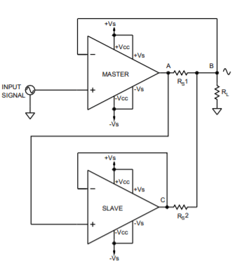
Non-inverting Parallel Amplifier Circuit
Power op amps in parallel operate something like batteries in parallel. If one battery is at higher voltage than the other, the battery with the higher voltage will try to force current into the battery with the smaller voltage. A similar thing can happen with power op amps in parallel. Since there is only one output voltage, one amplifier will try to sink or source current as necessary to force the other amplifier to the same voltage. That could result in a large amount of current flow from one amplifier into the other amplifier. The current might easily be larger than the load current and will exist whether or not there is any load current. The primary culprit that brings this on is offset voltage. Rs1 and Rs2 provide some feedback so that the two amplifiers share the load current almost equally. The larger the value of the balance resistors the smaller the current imbalance will be. But the choice of a value for Rs1 and Rs2 is a balancing act (no pun intended). As the value of these resistors increases so does the power dissipation in the balance resistors and this has a practical limit of about 10-15 watts. At the same time 150mV is needed to trigger the current limit function of the PAD121 Current Limit Accessory Module. So, for example, 10mΩ resistors provide a current limit trip point of 15A(I=0.15V/0.01Ω) for each amplifier (up to 30A total output current). And the offset voltage of the slave amplifier generates a total imbalance current of: Vos/Rs1 amps.
In the case of the PAD118 with a specified offset voltage up to ±5mV such an offset error will generate an imbalance current of ±0.5A. This means that one amplifier will supply 0.25A more than it should and the other amp will supply 0.25A less than it would if there were no offset at all. Compared to a full scale output current of 30A this imbalance current doesn’t seem to amount to much, but since the imbalance current is an offset, even when the load current is zero that total ±0.5A will still be there. One amplifier will source 0.25A while the other amplifier sinks 0.25A. As the load current increases to a point where it equals the imbalance current all the load current will come from one amplifier. As the load current increases further the load current will come from both amplifiers but will be imbalanced as mentioned above. Another effect of the imbalance current is to increase power dissipation in the amplifier that is supplying more current than it should while the other amplifier has less power dissipation than would be expected if the currents balanced perfectly.
For example, if the power supply voltages are ±50V and the output voltage is zero the imbalance current of 0.5A will result in a power dissipation of 12.5 watts in both amplifiers that wouldn’t exist if there were no offset voltage. Although the imbalance current could be as high as ±0.5A it will likely be much smaller since the typical offset of the PAD118 is only about 1mV. If this imbalance current magnitude seems too high the options are to either increase the Rs1and Rs2 or reduce the offset with an external balancing circuit. But keep in mind that increasing Rs1 and Rs2 will increase the power dissipation external to the amplifier and while this may be preferable to extra power dissipation inside the amplifier the overall result is still lower efficiency.
In addition, an error in current balancing is also created by a mismatch in the values of Rs1 and Rs2. The imbalance follows the mismatch percentage of Rs1 and Rs2. So, for example, if Rs1 and Rs2 are mismatched by 5% then the current imbalance due only to the mismatched balancing resistors will also be 5%. We recommend using 1% resistors like those you will find in our evaluation kits. This type of resistor is available from Isotek Inc., in a wide variety of values and tolerances.
Now we are prepared to show how the parallel amplifier circuit can be constructed using two EVAL118 evaluation kit circuit boards.
Figures 3a and 3b, below, show two schematics of the EVAL118 circuit board. One is labeled as the Master and the other as the Slave. The modifications necessary to create a parallel circuit are shown first in schematic form (in red) and then in Figures 4a and 4b how the modifications look physically on the actual board (in blue).
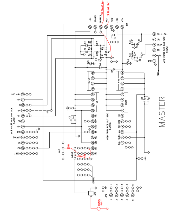
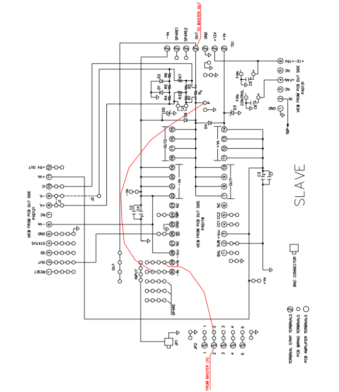
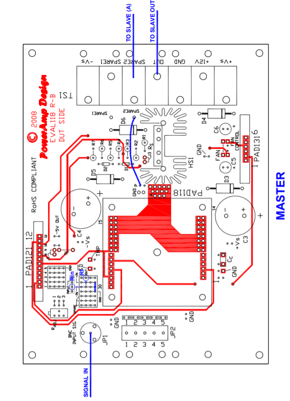
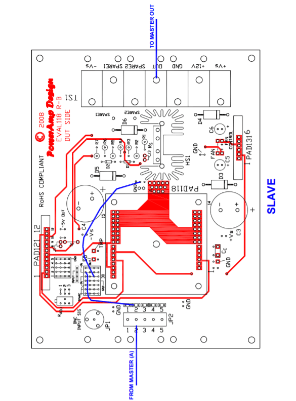
In figures 4a and 4b the schematics 3a and 3b have been given a more physical look as seen on the drawings of the circuit board for the EVAL118. The circuit has an inverting voltage gain of Rf/Rin as established by the components of the same names as seen on the Master drawing of the circuit board. All the components and jumper wires necessary for the parallel connections are drawn in blue. There are other equivalent ways of connecting the nodes, but the drawings show one convenient way to do it. For example, you could use a shielded cable to go directly from the Master at Node P on the circuit board to the input of the Slave.
Of course, other components will be necessary to program the current limit or make circuit variations; these drawings only address the basic connections for parallel operation. We hope these drawings give you the basic ideas from which you can make a more sophisticated circuit as your application demands. While the EVAL118 makes these connections easier than some other evaluation kit circuit boards the same ideas can be applied to all evaluation kit models.
Power op amps in parallel will never duplicate the performance of a single power op amp of similar capability, but parallel operation has the ability to fill in performance gaps not filled by current models.
AN-34
Force & Sense Application for Power Op Amps
Power Amp Design
Synopsis: The article details a force and sense application for power op amps using a familiar differential amplifier application for IC small signal circuits. Some familiarity with op amp circuits is assumed.
Power op amp circuits often require a substantial load current of several amps or even tens of amps. In addition, the load is often at some distance from the output of the power op amp. The resulting IR losses in the connections decrease the voltage across the load. When an accurate voltage at the load is required it is wise to use the power op amp as a differential amplifier to cancel the IR losses. The feedback to the amplifier will guarantee the required voltage is across the load.
In Figure 1, the amplifier is connected to the load through the inevitable parasitic wire resistances Rp1 and Rp2 in the output of the amplifier and also the ground connection of the load. Since the feedback to the amplifier is applied locally at the output of the amplifier the voltage drop created by Rp1 cannot be corrected. Also, no correction for the voltage drop across Rp2 is possible with this circuit.
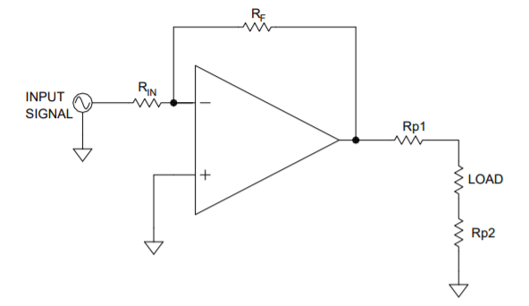
In Figure 2, the power op amp is configured as a differential amplifier. Due to the gain setting resistors 10R and R the circuit has a differential gain of 10. Any other gain would do as well. The circuit is inverting since the input signal is connected to the “minus” input of the amplifier. But the signal could just as well have been applied to the ‘plus” input of the amplifier for a non-inverting application.
“Force” and “Sense” are terms commonly referred to with this kind of circuit. The feedback connections to the amplifier are connected at the physical points to be controlled for voltage. In Figure 2, feedback to the inverting input of the power op amp is shown as “-Sense” and feedback to the non-inverting input of the amplifier is shown as “+Sense”. The output of the amplifier is referred to as “Force”.
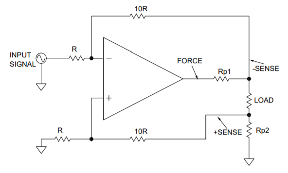
The circuit gives good accuracy with 1% resistors but it’s not difficult to find 0.1% resistors to improve the accuracy further. Either way, this differential circuit is a simple way to improve the accuracy of the voltage across the load compared with the circuit of Figure 1. With an output of 10 amps the voltage error across the load is 1 volt with 100mΩ of total parasitic resistance in the connections to the load. The circuit of Figure 2 will cancel that error with a minimal cost in components.
AN-38 (Rev C)
Fine Tuning Current Limit
Power Amp Design
Synopsis: By necessity only a few values of current limiting sense resistors can be supplied with evaluation kits. This application note shows how to achieve intermediate values of current limit with the resistors supplied in our evaluation kits.
Power Amp Design’s evaluation kits include a limited number of current limit sense resistor values. Typical values are 10mΩ, 15mΩ, 50mΩ and 100mΩ, as provided in the EVAL117. Whether the PAD125 Current Limit Accessory Module is used or the built-in current limit circuit is used the typical values of sense resistor provide only a limited range of current limit set points. It is often desirable to achieve some intermediate value.
Fortunately, many of the evaluation kits are designed with locations where additional resistors can be added to the circuit to modify the current limit set point using a simple voltage divider network.
In Figure 1, the schematic of the EVAL117 is shown. Although each evaluation kit model has a somewhat different circuit, the components around the Rs resistor are the same for amplifiers with 4-wire current limit scheme and this same technique can be used with other evaluation kits or, indeed, your production circuit.
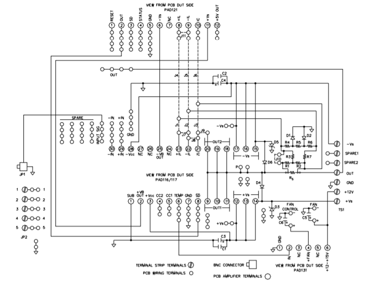
Circuit Diagram of the EVAL117 Evaluation kit
In the EVAL117 none of the components R1-R7 or D1, D2 are supplied. These components are used to implement a fold-over current limit scheme. But R1, R2 can also be used to modify the current limit set point that would otherwise be determined by Rs alone.
For example, let’s assume that the PAD125 Current Limit Accessory Module is being used in your circuit and you want to current limit at 5 amps. Since the current limit sense voltage of the PAD125 is 150mV, Rs would normally be determined by
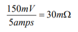
A 30mΩ resistor value is not included in the EVAL117 evaluation kit, but we can still achieve the 5 amp current limit (or any other intermediate value). A suitable method for determining circuit component values to achieve a 5 amp current limit follows:
- Select the next higher sense resistor provided; in this case a 50mΩ resistor (provided in the EVAL117 kit).
- Assign a value of 50Ω to R1 as this will simply the arithmetic by reducing loading of the circuit.
- Find the voltage developed across the selected Rs by the desired current limit value.
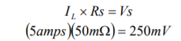
where IL is the desired current limit and Rs is the selected sense resistor value, and Vs is the voltage developed across the sense resistor.
4. And, finally, solve for the value of R2.
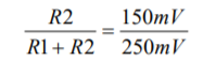
where 150mV is the sense voltage needed to trip the current limit circuit and 250mV is the voltage developed across the 50mΩ sense resistor that was selected.
R2 solves to be 75Ω.
To complete the circuit remove jumper J10 (or J3 in some evaluation kit models) and install a wire to jumper R3. Now, when 5 amps flows through Rs 150 mV will appear across R2 and the PAD125 will shut down the PAD117 at 5 amps output. It is the voltage across R2 that now provides the input voltage to the PAD125. Other ratios of R1 and R2 will, of course, give different current limit trip points. Since the values of Rs are so small, even small values of R1 and R2 will not much affect the accuracy of current limit set point and can probably be ignored since even the small values in this example are on the order of 1000 times greater that the sense resistor. The input impedance to the PAD125 is high and so this can also be neglected.
The final check you should make is for the power dissipation in Rs. In our example up to 5 amps could flow in Rs. The maximum power dissipation in Rs is then

Up to 8 watts dissipation in the heat sink for Rs is permissible so this total solution works.
This same technique also works when the internal current limit circuit is used in place of the PAD125 (for those models with an internal current limit option). The difference is that the internal current limit has a different sense voltage (approximately 0.65 volts) and is temperature dependent and not a precise as that of the PAD125.
Thus far we have discussed fine tuning the current limit for models having a 4-wire current limit capability. The 4-wire current limit scheme is characterized by the amplifier having current limit pins called +IL, -IL and IC. You can see these pins in the EVAL117 schematic where the pin-out of the PAD117 is shown.
Some other amplifier models do not have the 4-wire current limit capability and there is only one pin used for the current limit function and this pin is called IL. An example is the model PAD138. Below in Figure 2, is the schematic of the EVAL138, the evaluation kit for the PAD138.
Fine tuning of the current limit is still possible but the arithmetic is a little more difficult. In the schematic of the EVAL138 you will note that R1 and R2 are present, in parallel with Rs as was the case in the EVAL117 previously described. But in the case of the EVAL138 the divider network is loaded by the internal stage current of the PAD138 that is dumped into the current limit network during current limit. By the connections made in the EVAL117 this loading current was dumped directly into the load and therefore did not load the current limit sensing resistor network. These same connections are not possible in the case of the EVAL138 and PAD138 due to the fact that there is only one pin assigned to the current limit function. But this just makes the calculation more difficult and somewhat less precise.
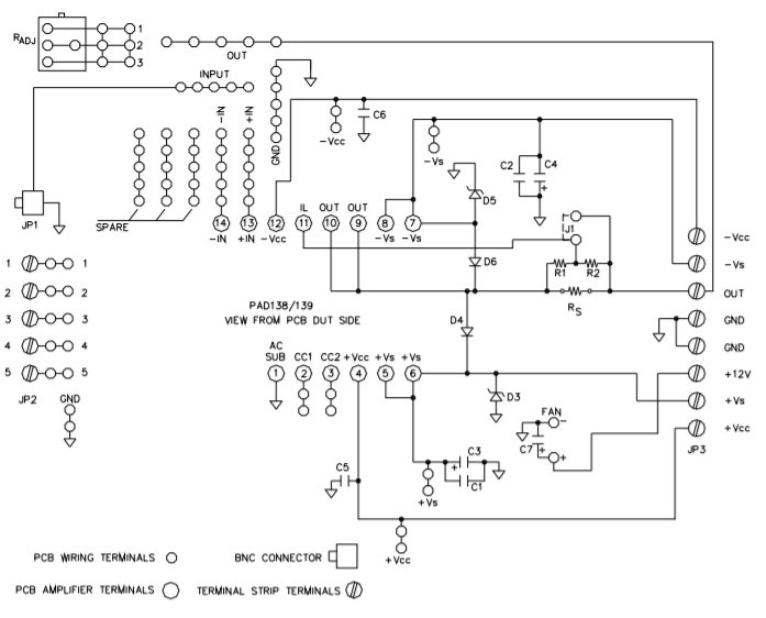
EVAL138 Schematic
In the EVAL138 several current limiting resistors are provided: one 100mΩ, one 200mΩ and one 500mΩ. The current limit circuit is not a precision circuit but the approximate current limit value can be determined by:

Where IL is the desired current limit value and Rs is the current limit sense resistor value
Using the supplied current limit sense resistors (Rs) the current limit values obtainable are:
RS ≈IL
100mΩ 7.0A
200mΩ 3.5A
500mΩ 1.4A
But suppose the desired current limit point is 2A. The values supplied in the EVAL138 will not give you a 2A current limit but we can achieve that with the R1, R2 divider.
A suitable method for determining the values of R1 and R2 in Figure 2 is to first determine the largest supplied value of Rs that would give you something less that the current limit value you desire. For example, if you wanted a current limit value of 2A you would select the 500mΩ resistor supplied in the EVAL138 kit. Next, assign R1 a value of 50Rs (this assignment keeps the power dissipation of R1 within the ¼ watt rating of common resistors) and solve for R2 in the following equation:
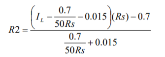
Where IL is the desired current limit value and Rs is the current limit sense resistor value. The 0.015 constant is the average loading current from PAD138 that is dumped into the current limit resistor network during current limit. For other amplifiers this number will probably be different. The 0.7 constant is the current limit sense voltage set by the internal sensing circuit. This constant may also vary a little with other models.
In this example, when a current limit of 2A is desired Rs is 500mΩ, R1 is 25Ω (50Rs) and R2 is 6.477Ω. Standard 1% values of 24.9Ω and 6.49Ω are adequate substitutions.
The exact desired value of Rs is often hard to find and this technique can be used to fine tune the current limit set point to most any value desired.
AN-40
Using the CJS01 Cage Jack Strip
Power Amp Design
Synopsis: This article provides details for using the CJS01 in the assembly operation of circuit boards.
It can be difficult or even impossible to remove power op amps from the mother board should one have to be replaced, especially in boards with platedthrough holes. Attempting to remove the amplifier after soldering the pins can result in damaging the amplifier or circuit board or both. It is convenient therefore for the amplifier to be plugged into a socket.
The CJS01 is a 32 position strip of individual socket receptacles (cage jacks) just for that purpose. The CJS01 consists of two parts: the carrier strip and the individual sockets. Together the two parts are both the socket and an assembly aid.
The various amplifier models have different pin counts. The CJS01 can be easily cut to the required length with wire cutters. The 32 pin count strip can usually be cut into enough pieces to meet the total pin count of most amplifier models.
The assembly procedure is straight forward.
- Cut the CJS01 into sections long enough to match the pin count on each side of the amplifier.
- Insert each cut length into the corresponding holes in the circuit board from the same side of the circuit board that the amplifier will plug into.
- Provide some method where the CJS01 section is held tightly agains the circuit board
- Solder the sockets from the other side of the board
- Remove and discard the carrier.
In applications where the CJS01 is used with circuit boards having platedthrough holes it is often helpful first to coat the area with flux before inserting the cut strips. A flux pen is most convenient for this operation such as the Kester #2331-zx. The additional flux will help the solder flow all the way to the other side of the board so that solder will flow under the head of the socket.
In many of the amplifier models several of the amplifier pins are connected together to improve the current handling capacity. The sockets therefore will be connected to common metal. These pads may be large and extra heat and/or a larger soldering iron tip may be needed to provide the heat necessary to melt all the solder on the pad. Adding the flux as mentioned above helps the solder flow over the entire pad without overheating the pad and insures that the solder flows to the other side of the board. For amplifier models with double rows of pins insert all the sockets in the double row before soldering.
The CJS01 datasheet provides dimensional information that should be used to design the circuit board pads. See figure 1 below for a recommended geometry for individual connections. As mentioned above, the pads may be connected with common metal where paralleled pins are required by the amplifier model.
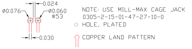
The CJS01 is loaded with Mill-Max cage jacks model 0305-2-15-01-47-10-0. You may also purchase directly from Mill Max the model 703-93-132-47- 052100 which is similar to the CJS01.
AN-42
Using Evaluation Kits to Implement a Current Source Circuit
Synopsis: Power Amp Design’s evaluation kits are normally configured to build voltage control application circuits, but it is also possible to build a current mode (transconductance) circuit as detailed in this article. Some knowledge of op amp circuit theory is assumed.
Operational amplifiers are designed to be voltage controlled circuits (voltage in, voltage out). Power Amp Design’s evaluation kit circuit boards are designed with voltage control circuits in mind. However, a transconductance (voltage in, current out) application circuit can be constructed as well using an evaluation board.
Operational amplifiers are designed to be voltage controlled circuits (voltage in, voltage out). Power Amp Design’s evaluation kit circuit boards are designed with voltage control circuits in mind. However, a transconductance (voltage in, current out) application circuit can be constructed as well using an evaluation board.
The Howland current pump is the easier of the two circuits to implement using the evaluation kit board because the location of the current sensing resistance, Rs, is similar in both the voltage control and Howland current control application circuits. Therefore, this article will focus on the Howland current pump although the operation of the floating load current source will also be discussed briefly. Evaluation boards can also be adapted to the floating load current source but this circuit is much more difficult to construct and no details as to how to do this will be offered.
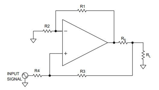
Simple Howland Current Pump Circuit (non-inverting)
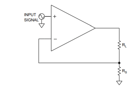
Simple Floating Load Current Control
In many applications the load must be grounded because of the way the load is physically constructed. The Howland current pump of Figure 1 is a suitable circuit for such circumstances. The scaling of the circuit is easy. First note in Figure 1 that R1 and R3 are to be the same values and R2 and R4 are the same values as well. As such the scaling of Figure 1 follows the equation:
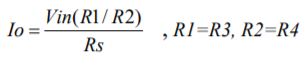
For example, if R1 and R3 are each 1kΩ , R2 and R4 are each 10kΩ and Rs is 100mΩ then 10V of input voltage will result in 10A of current in RL, or 1 amp output per volt of input, 1A/V.
As a practical matter, useful values of Rs between 10mΩ and 100mΩ work best, and the larger values work better overall. The limits of power dissipation in the sense resistor, Rs, must be kept in mind, because the power
dissipation limit with the heat sink provided in the evaluation kit is 8-10 watts.
The selection of the sense resistor value is always a trade-off between power dissipation and circuit accuracy. The offset voltage of the amplifier appears across the sense resistor (multiplied by the circuit gain, if greater than 1) and so introduces a current error in the load.
For example, if the amplifier has an offset voltage of 5mV (including temperature drift) and the sense resistor chosen is 10mΩ, the current in load produced by the offset voltage will be simply
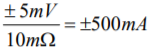
and this current will either add to or subtract from the current in the load demanded by the input voltage depending on the polarity of the offset voltage. As the value of the sense resistor increases the error current due to offset voltage decreases, but the power dissipation in the sense resistor increases.
There is another error current, namely, the current feedback in R3, but as a practical matter this current is usually negligible and can be ignored in most cases.
As you would expect, the tolerances of the various resistors also contribute to the error in the output current. Using 1% resistors tolerances usually gives satisfactory performance for gain error, but tighter tolerance resistors are not hard to find. Feedback resistor tolerances of 0.1% are easily obtainable. A sense resistor tolerance of 0.5 to 1% are also obtainable. The sense resistors supplied in the evaluation kits are in that range. Kelvin sense resistors are needed for current source applications due to the low values of the sense resistors in the circuits.
The Howland current pump can just as easily be configured for an inverting signal application by just reversing the connections to the inputs. Figure 3 below shows a schematic for an inverting Howland circuit.
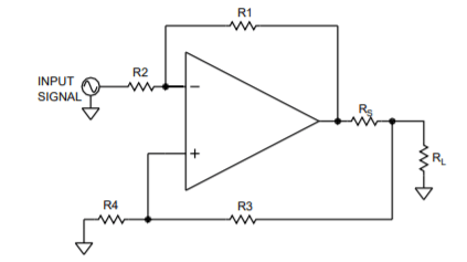
A simple inverting Howland Current Pump
Likewise, the floating load current source of Figure 2 can also be reconfigured for inverting operation. See Figure 4 below.
The output current of Figure 4 is:
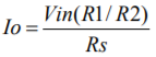
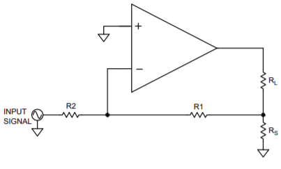
Inverting Floating Load Current Source
The final step is to implement a Howland current pump circuit (non-inverting) on an evaluation board. In Figure 5 below resistors R1, R2, R3 and R4 of Figure 1 have been added to the evaluation board. See the components in the magenta color. R1 and R3 of Figure 1 have been inserted into the holes in the board that connect these resistors to the sense pins of the Kelvin sense resistor Rs. The other ends of the resistors are connected with flying wires to the bread boarding area. Also in the magenta color are resistors R2 and R4 to complete the current pump circuit. Figure 5, showing a modified EVAL117 board is a typical example to follow. Other evaluation kits have similar connections available. You can consult the schematic of the various models of evaluation kits. As time goes on Power Amp Design is converting our evaluation kits to include feedback points in the design of our evaluation kits to simplify implementing the Howland current pump circuit.
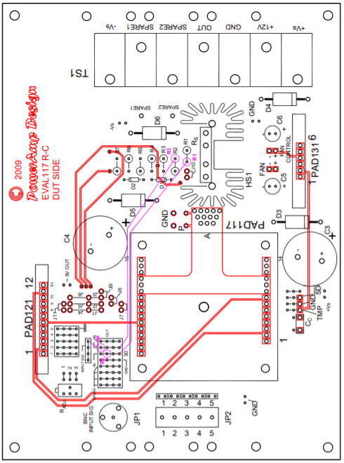
EVAL117 with Howland Current Pump Modifications (magenta)