AN-32
Using Evaluation Kits to Implement Parallel Operation
Power Amp Design
Synopsis: How to use two or more evaluation kits to connect power op amps for parallel operation.
An increasingly popular application calls for paralleling power op amps either to increase the available output current or sharing the power dissipation among two or more amplifiers. In this article we will show the top level schematic for connecting power op amps in parallel and also how to use two or more evaluation kits to implement parallel operation. For examples, we will refer to the EVAL118 evaluation kit for the PAD118 High Power Operational Amplifier since this is a common amplifier model used for parallel operation.
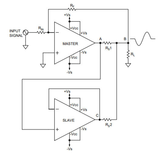
INVERTING PARALLEL OPERATION
Figure 1 illustrates the top level schematic connections for two amplifiers in parallel. The circuit is inverting. The output of master amplifier (node A) is also the input signal to the slave amplifier connected as a unity gain follower. Notice that the feedback to gain setting resistor RF is connected to the output of the combined circuit (node B) whereas the feedback for the slave amplifier (node C) is connected directly to the output of the slave. Between nodes A and B and also nodes C and B you will notice balance resistors Rs1 and Rs2. These resistors help insure that the amplifiers share the load current for the inevitable case where the slave has some offset. The master amplifier can, of course, drive more than one slave. The slave connections can be repeated for additional slave amplifiers.
When the EVAL118 is not used for parallel operation Rs1 (Rs on the circuit board) is intended as a current sense resistor used in conjunction with the PAD121 Current Limit Accessory module. But for this parallel application the current sense resistor will double as a balance resistor. Later we will show how these balance resistors can also be used to set the current limit trip point. See the datasheet for the PAD121 for complete details on its operation.
In the case of the PAD118 power op amp, a current limit function is not built-in but relies on the PAD121 to perform that function. The EVAL118 supports the PAD121 with a plug-in slot. The PAD121 can be programmed to select one of several modes of current limit operation. Basic operation of the PAD121 is pre-wired on the EVAL118 circuit board with jumpers that connect its inputs to Rs1 (Rs on the circuit board) as shown in the above schematics. When the output current of the amplifier reaches the set point (±150mV across the current sense resistor Rs) the PAD121 shuts down the PAD118. Although it is possible to use only one PAD121 to control both amplifiers in parallel we recommend that each amplifier in parallel have its own PAD121. With a little planning Rs1 and Rs2 can serve as both a current limit sense resistor and a balancing resistor. Typical values that serve both functions are 10mΩ and 15mΩ, but other values may work equally well depending on the details of your circuit.
While the inverting configuration is the most common application it is also possible to operate power op amps in parallel with non-inverting circuits. Figure 2 below shows a similar schematic to Figure 1 but with both the master and slave as non-inverting amplifiers. The non-inverting parallel circuit occurs most frequently in low voltage amplifier applications where the input signal is of sufficient amplitude but needs to be boosted in output power capability. Driving low voltage motors is an example where power supply voltages of ±15V might be used.
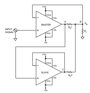
Non-inverting Parallel Amplifier Circuit
Power op amps in parallel operate something like batteries in parallel. If one battery is at higher voltage than the other, the battery with the higher voltage will try to force current into the battery with the smaller voltage. A similar thing can happen with power op amps in parallel. Since there is only one output voltage, one amplifier will try to sink or source current as necessary to force the other amplifier to the same voltage. That could result in a large amount of current flow from one amplifier into the other amplifier. The current might easily be larger than the load current and will exist whether or not there is any load current. The primary culprit that brings this on is offset voltage. Rs1 and Rs2 provide some feedback so that the two amplifiers share the load current almost equally. The larger the value of the balance resistors the smaller the current imbalance will be. But the choice of a value for Rs1 and Rs2 is a balancing act (no pun intended). As the value of these resistors increases so does the power dissipation in the balance resistors and this has a practical limit of about 10-15 watts. At the same time 150mV is needed to trigger the current limit function of the PAD121 Current Limit Accessory Module. So, for example, 10mΩ resistors provide a current limit trip point of 15A (I=0.15V/0.01Ω) for each amplifier (up to 30A total output current). And the offset voltage of the slave amplifier generates a total imbalance current of: Vos/Rs1 amps.
In the case of the PAD118 with a specified offset voltage up to ±5mV such an offset error will generate an imbalance current of ±0.5A. This means that one amplifier will supply 0.25A more than it should and the other amp will supply 0.25A less than it would if there were no offset at all. Compared to a full scale output current of 30A this imbalance current doesn’t seem to amount to much, but since the imbalance current is an offset, even when the load current is zero that total ±0.5A will still be there. One amplifier will source 0.25A while the other amplifier sinks 0.25A. As the load current increases to a point where it equals the imbalance current all the load current will come from one amplifier. As the load current increases further the load current will come from both amplifiers but will be imbalanced as mentioned above. Another effect of the imbalance current is to increase power dissipation in the amplifier that is supplying more current than it should while the other amplifier has less power dissipation than would be expected if the currents balanced perfectly.
For example, if the power supply voltages are ±50V and the output voltage is zero the imbalance current of 0.5A will result in a power dissipation of 12.5 watts in both amplifiers that wouldn’t exist if there were no offset voltage. Although the imbalance current could be as high as ±0.5A it will likely be much smaller since the typical offset of the PAD118 is only about 1mV. If this imbalance current magnitude seems too high the options are to either increase the Rs1and Rs2 or reduce the offset with an external balancing circuit. But keep in mind that increasing Rs1 and Rs2 will increase the power dissipation external to the amplifier and while this may be preferable to extra power dissipation inside the amplifier the overall result is still lower efficiency.
In addition, an error in current balancing is also created by a mismatch in the values of Rs1 and Rs2. The imbalance follows the mismatch percentage of Rs1 and Rs2. So, for example, if Rs1 and Rs2 are mismatched by 5% then the current imbalance due only to the mismatched balancing resistors will also be 5%. We recommend using 1% resistors like those you will find in our evaluation kits. This type of resistor is available from Isotek Inc., in a wide variety of values and tolerances.
Now we are prepared to show how the parallel amplifier circuit can be constructed using two EVAL118 evaluation kit circuit boards.
Figures 3a and 3b, below, show two schematics of the EVAL118 circuit board. One is labeled as the Master and the other as the Slave. The modifications necessary to create a parallel circuit are shown first in schematic form (in red) and then in Figures 4a and 4b how the modifications look physically on the actual board (in blue).
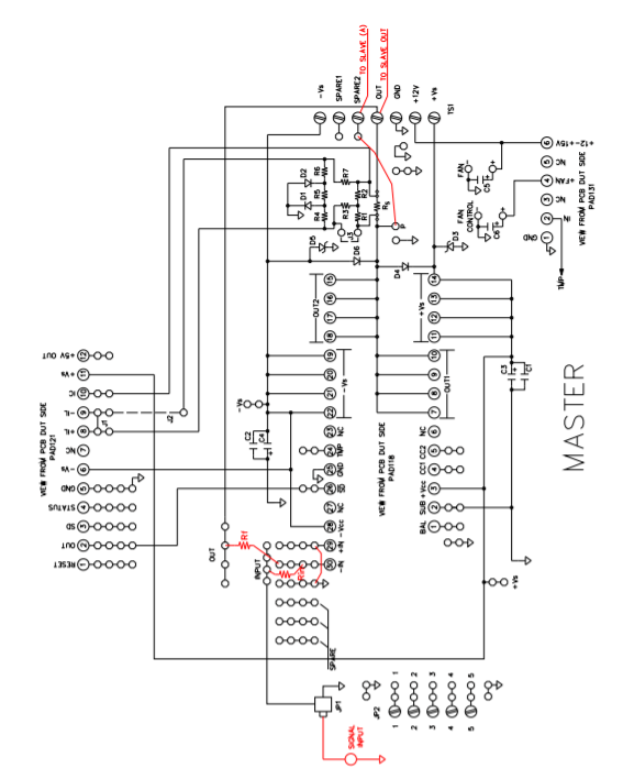
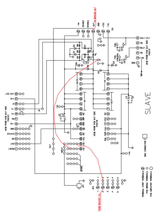
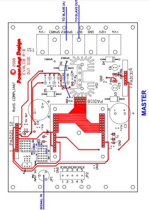
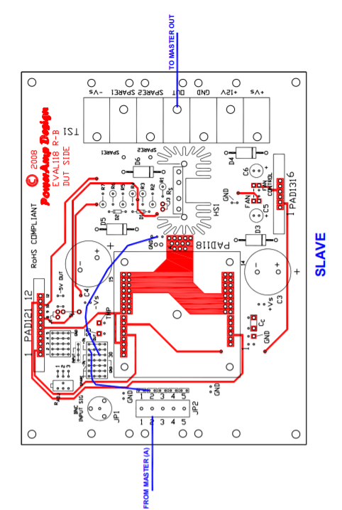
In figures 4a and 4b the schematics 3a and 3b have been given a more physical look as seen on the drawings of the circuit board for the EVAL118. The circuit has an inverting voltage gain of Rf/Rin as established by the components of the same names as seen on the Master drawing of the circuit board. All the components and jumper wires necessary for the parallel connections are drawn in blue. There are other equivalent ways of connecting the nodes, but the drawings show one convenient way to do it. For example, you could use a shielded cable to go directly from the Master at Node P on the circuit board to the input of the Slave.
Of course, other components will be necessary to program the current limit or make circuit variations; these drawings only address the basic connections for parallel operation. We hope these drawings give you the basic ideas from which you can make a more sophisticated circuit as your application demands. While the EVAL118 makes these connections easier than some other evaluation kit circuit boards the same ideas can be applied to all evaluation kit models.
Power op amps in parallel will never duplicate the performance of a single power op amp of similar capability, but parallel operation has the ability to fill in performance gaps not filled by current models.