AN-22
Single Supply Operation with Power Op Amps
Power Amp Design
Synopsis: The article outlines the problems and solutions for operating power op amps with a single high power supply voltage. Several application circuits are proposed that may help the user reduce system costs while maintaining high performance. Some familiarity with op amp circuits is assumed.
Although this article assumes some knowledge of operational amplifiers it may be beneficial for some readers to review a brief refresher on op amp theory. Other readers may feel free to skip to page 3.
Today’s operational amplifiers, whether constructed from discrete components or a monolithic chip, approach many of the characteristics of the ideal differential gain block of Figure A. The ideal differential gain block is characterized by infinite gain and bandwidth, infinite input impedance, zero output impedance and zero differential input error. These characteristics imply that the overall performance of an application circuit is determined by the external components connected to the op amp.
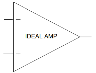
It is easier to analyze any op amp circuit if you keep the ideal characteristics in mind and also remember that the action of any op amp circuit is to swing the output to such an amplitude and polarity that the two inputs (+ and -, noninverting and inverting respectively) are at the same voltage. The op amp accomplishes this through feedback, i.e. the external components tied between the inputs and the output of the op amp. The inverting input is so named because a positive going signal (for example) at this input forces the output of the op amp to be negative going. The non-inverting input does the opposite; a positive going input signal on the non-inverting input forces the output to also be positive going. The circuit in Figure B, for example, can be easily analyzed using these principles.
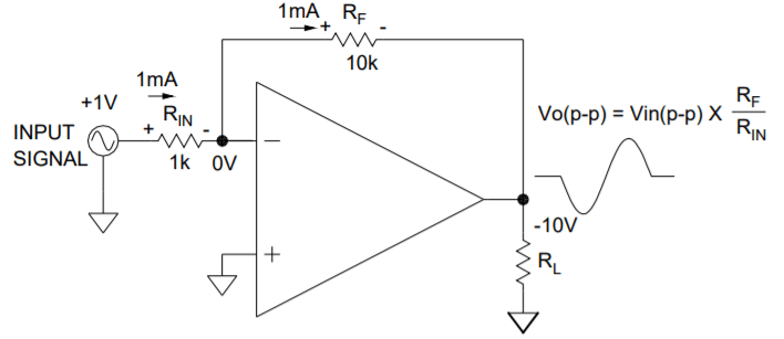
Note that the non-inverting input of the amplifier is grounded (zero volts). Since the ideal amplifier has zero differential error the inverting input must also be at zero volts (virtual ground). If the input voltage is +1V then 1mA flows into the inverting node (-). Remember that for the ideal amplifier no current flows into the inputs (infinite input impedance). The entire 1mA therefore must flow into RF (10k). The resulting voltage at the output of the amplifier must be -10V (1mA X 10k). This is the basic inverting amplifier configuration.
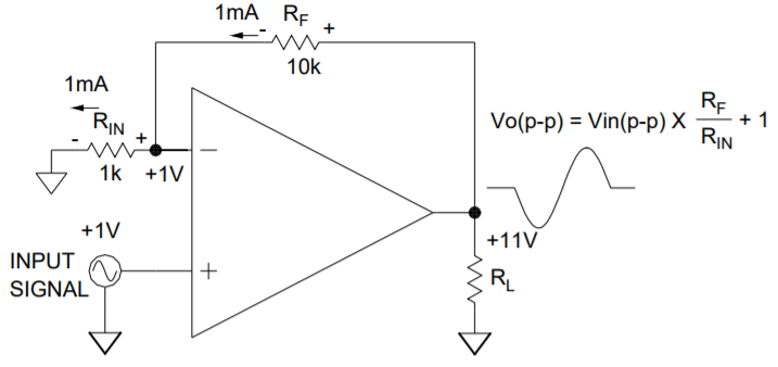
A similar analysis can be performed with an input signal tied to the noninverting input of the op amp. In Figure C, +1V is tied to the + input of the op amp. As before, since there is no differential error between the inputs of the op amp, the inverting input must also be at +1V. The output of the amplifier swings in a direction (polarity) and amplitude to make this so. The +1V causes 1mA to flow into ground from the inverting node. The same 1mA therefore flows through RF (10k) developing 10V in doing so. Since one end of RF is tied to +1V the other end must be at +11V and this accounts for the signal gain of +11 as opposed to the inverting amplifier signal gain in Figure B of -10 using the same values for RIN and RF. This is the basic non-inverting amplifier configuration.
These simple concepts will help in analyzing any op amp circuit.
If you skipped the op amp primer you can pick up the discussion here:
From the very beginning operational amplifiers have been powered by positive and negative power supplies ─ ±15 Volts, for example, is very common. There are good reasons for this: the dual supplies overcome possible biasing problems with the internal design of the op amp and, from an external point of view, it allows the output of the amplifier to reach zero volts. The dual power supplies also allow for reversing of a grounded motor load, for example. The dual supply approach works very well but there is a cost impact as well.
In the last several years a plethora of small signal op amps have reached the market that can operate on a single power supply. Some of these designs are “rail to rail”, or RRIO, standing for rail to rail input and rail to rail output; i.e. both the input and output voltages can swing to the power supply voltages. In the case of the output specification “rail to rail” is really only an approximation. As the op amp output transistors sink or source current some voltage drop necessarily occurs. At the inputs of the op amp, however, “rail to rail” is actually achievable.
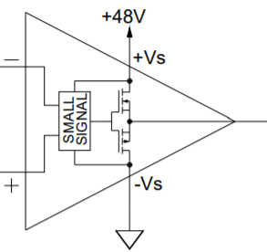
In the case of power op amps the situation is a little different. As opposed to the milliamp output of its small signal cousins the power op amp can provide an output of a few amps to several tens of amps depending on the model. Power op amps usually do not operate RRIO although a few IC power op amp models on the market do have an input common mode range that includes the negative supply voltage (see discussion below).
Thus far Power Amp Design is unique in this way. To date Power Amp Design has two RRIO models, the PAD117 and the PAD127. Like their small signal brethren these two models cannot supply output current without dropping some voltage, but the PAD117, for example, can supply 15 amps with only a 1.5 volt drop from the power supply voltage. The PAD127 can do likewise with a 30 amp output.
The major reasons for operating a power op amp with a single supply voltage are system cost and/or weight. While providing ±15 volts for a small signal op amp may not entail much cost a second power supply that can provide 10 or 20 amps at 50 or 100 volts would be of considerable expense and weight.
Two important op amp specifications need to be examined when considering a power op amp for a single supply application: input common mode range and output swing under load.
The input common mode range specifies how closely the inputs of the op amp can approach the power supply rails and still have the op amp operate correctly. In every op amp circuit the two inputs are maintained at virtually the same voltage owing to feedback in the external circuit. When the input voltage is pushed beyond the common mode range of the amplifier the internal biasing requirements of the op amp are no longer met and the output of the amplifier cannot swing to the correct output voltage. Often the common mode range is not symmetric, i.e. the inputs may be allowed to swing within 2 volts of the negative power supply voltage, but only within 5 volts of the positive power supply voltage. Some amplifiers allow the inputs to go all the way to the negative power supply voltage and these designs are often referred to as having a “common mode range that includes ground”. Power Amp Design’s model PAD117 is such an amplifier.
The output swing capability specification of the power op amp is also important. At high output current the output voltage of an ordinary power op amp may drop as much as 7 volts from the power supply voltage. If, for example, a single supply application is powered by +48 volt power supply the output swing may be limited to 34 volts total owing to the 7 volt drop from each supply rail (+48V and ground ─ the negative supply). The voltage drop from each power supply rail limits the output swing and reduces the efficiency of the circuit. The wasted power ends up as a higher amplifier operating temperature.
In the most usual single supply configuration (Figure 1) a power op amp is powered by a positive power supply (+VS) and the negative power supply connection (-VS) is tied to ground (common). A common design challenge with this configuration is that the non-inverting input must be floated to some positive voltage to meet the common mode requirement of the op amp. A few power op amps on the market have a common mode range that includes the negative supply voltage, but this is rare. From a biasing point of view the output stage doesn’t care if only one polarity of power supply voltage is available, but the input stage does care unless especially designed so that its common mode range includes the negative supply voltage.
At this point a distinction needs to be addressed. Traditionally, op amps have only two power supply connections, +VS and –VS. Most of the op amps on the market today are powered in this way. Consequently “single supply” has come to mean that the entire op amp must operate from these two power inputs, one of which is grounded for single supply operation. But, for power op amps, all that is really needed is for the output stage of the op amp to operate from a single supply voltage since eliminating one high power supply is where the cost savings come from. The small signal stages of the op amp are not required to operate from a single supply voltage even if the amplifier’s output stage is.
Power Amp Design models have significant advantages when applied to single supply applications when compared to most monolithic or hybrid power op amps. Power Amp Design models usually operate from four power supply voltages, +Vcc, -Vcc, which are connected to the amplifier’s small signal stages, and +Vs and -Vs which are connected to the amplifier’s output stage. In many or most applications +Vcc and +Vs are tied together and, likewise, -Vcc and –Vs are connected. But these connections are not required. (The four power supply connections are not provided in the RRIO models PAD117 and PAD127 as this feature is unnecessary for RRIO designs.)
Let’s look at an application (Figure 2) where bipolar system power supplies are available to power the small signal stages of the amplifier but the output stage is powered from a single high power supply.
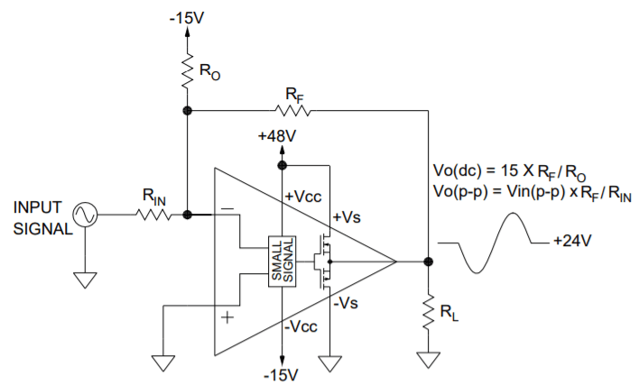
The circuit in Figure 2 takes advantage of the four power supply voltages available in Power Amp Design op amp models. The figure shows the power supply connections to the small signal (input) stages of the op amp and also the power connections to the output stage MOSFET transistors. While the positive power supply connections are connected together (+VCC and +VS) the negative power supply connections (-VCC and -VS) are not. Instead, -VCC is connected to the system -15V power supply and the output stage -VS is tied to ground. Connecting the system -15V power supply to the small signal stage of the power op amp is usually not a burden since the small signal stages of the op amp typically draw only a few milliamps.
The alternate connection for -VCC provides two benefits. One benefit is that the common mode input voltage range specification is met. The non-inverting input is grounded and thus is 15V from the negative supply voltage (-VCC). Some op amp output stage designs (PAD128, for example) benefit from a second and less obvious advantage: the drive to the output stage transistor connected to -VS has an additional 15V of drive voltage available. Thus the output transistor can drive the output voltage much closer to ground than would otherwise be possible.
Another feature of the circuit in Figure 2 utilizes the -15V to generate a +24V offset at the output of the amplifier. Thus any AC input signal will swing plus and minus about the +24VDC level at the output of the amplifier. If the -15V wanders with load or temperature the output of the amplifier will wander as well. It is therefore best that the -15V be either regulated and temperature stable or that it be regulated to some other lower voltage that is stable.
The amplifier has some offset voltage that drifts over temperature. For power op amps typical offset voltages range from 1 to 5 mV and drifts up to 50µV/°C. The amplifier’s offset voltage is magnified at the output by the DC gain of the amplifier as set by the feedback network. Any offset externally set by the circuit should be at least as stable as the offset of the amplifier.
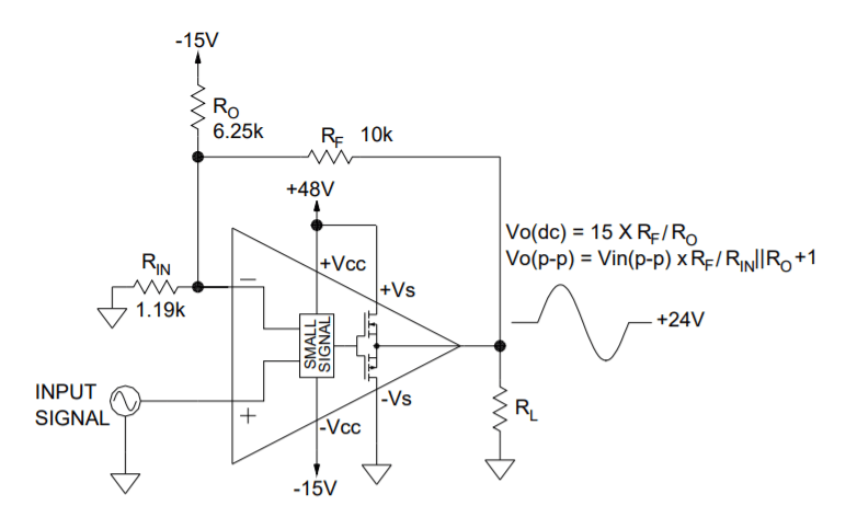
Figure 3 below shows another circuit similar to the inverting circuit of Figure 2, but non-inverting. Mathematically this circuit is a little more complicated since RO and RIN appear in parallel (the || symbol in the equation) in calculating the gain of the circuit. Example resistor values are given to illustrate a signal gain of 11 while the output is offset to a DC value of +24V.
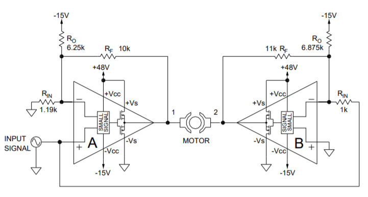
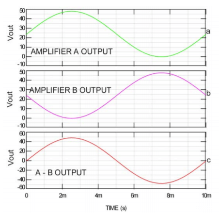
In Figure 4 below, the ideas of Figure 2 and Figure 3 are combined into a bridge circuit to drive a brush motor. While Amplifier A’s output is going positive (Figure 5a) Amplifier B’s output is going negative (Figure 5b). The result is that up to 96V p-p (Figure 5c) is available to drive the motor from a single +48V power supply (neglecting voltage drops across the output stage of each amplifier). The signal gain of each amplifier is 11 and the total signal gain that appears across the motor is 22 for the values shown. Another way to interpret the output of the bridge circuit is that the motor can be driven to 100 % RPM in either direction depending of the polarity of the input voltage.
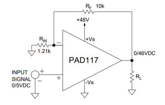
In another system there may be no negative small signal power supply available. In the simplest case a unipolar input signal results in a unipolar output voltage from the amplifier. In Figure 6, a 0/5V signal results in a 0/46V output voltage from a PAD117 RRIO power op amp from Power Amp Design. With no load current the PAD117 output can reach zero volts. The input is also rail to rail capable so an input voltage of zero volts does not violate the common mode range of the amplifier. This is an application where the RRIO power op amp is very helpful since few external components are needed to make the amplifier work properly.
Still another circuit, both more versatile and more complicated, is shown in Figure 7, below. In this circuit a charge pump circuit converts the high voltage positive supply voltage into a negative low voltage reference voltage suitable for establishing a +24 volt offset at the output of the power amplifier.
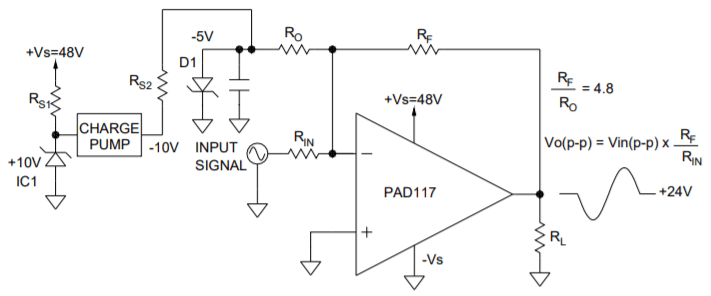
The amplifier in Figure 7 is a PAD117 from Power Amp Design and is a RRIO design. The non-inverting input can be grounded and not violate the input common mode range of the amplifier. The gain of the amplifier stage is easily varied as is the output offset voltage by adjusting RF, RIN and RO. For maximum output offset stability D1 is a reference integrated circuit that acts like a zener diode, a National LM4040DIM3-5.0, for example. The charge pump voltage inverter circuit is constructed using a Microchip TC7660 integrated circuit. The TC7660 requires two external capacitors (not shown) to make the voltage conversion.
Summary
Traditionally op amps have only two power terminals. Since one power terminal is grounded for single supply applications some sort of input biasing scheme must be used to satisfy the input common mode voltage requirements
of the op amp. While it is possible to overcome this problem with an input stage design that has a common mode voltage range that includes the negative supply voltage this type of design is rare for power op amps. Overall it is more beneficial for a power op amp to have four power terminals where the small signal stages of the power op amp and the output stage are powered separately so that the input stages of the op amp can take advantage of the low voltage power supplies that may already be available in the system. It is also more beneficial to use power op amps that are of a RRIO design since this design is easier to bias in single supply applications and provides a more efficient use of the power supply voltages available since the output of the RRIO design swings much closer to the supply voltages than any other power op amp designs. To date Power Amp Design is the only manufacturer with RRIO power op amp designs available.