AN-16
PCB Layout Guidelines for High Voltage Amplifiers
Power Amp Design
Synopsis: Standard company design rules for printed circuit boards may not meet the requirements for high voltage amplifiers manufactured by Power Amp Design. The article proposes PCB geometries consistent with successful field applications for high voltage amplifiers.
As circuit size shrinks it may not be practical for today’s high voltage amplifiers to adhere to the old PCB trace spacing design rules of yesteryear. As far back as 1980, Sandia National Laboratories did a study* to determine new trace spacing rules that would be reliable. Sandia found the then current standards wanting.
Although the printed circuit geometries presented below do not always follow the recommendations of Sandia they do follow Sandia’s data. The key difference between the recommendations of Power Amp Design and Sandia’s data is that the data from Sandia refers to an altitude of 25,000 feet and near 100% humidity. Altitude is the biggest player in determining reliable trace separations, safe spacing growing larger as the atmospheric pressure drops at higher altitudes. Power Amp Design’s suggested geometries should prove reliable to an altitude of 10,000 feet assuming a clean PCB and a normal (for the altitude) atmosphere. Other operating conditions may require the user to provide conformal coatings, a pressurized system containing the amplifier, or other means to prevent breakdown between adjacent amplifier pins and the user’s supporting circuitry carrying voltage differentials of 500V or more.
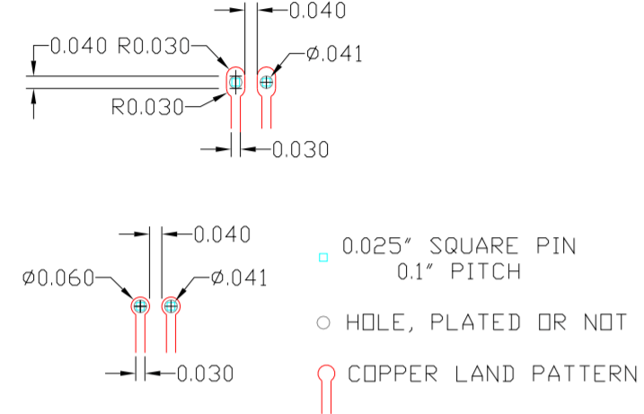
The most conservative approach is to solder the amplifier into the PCB. The geometries in Figure 1 illustrate the recommended PCB layout geometries for this method. Either geometry shown will work. Solder mask may be applied in addition.
*IPC-TP-333, Voltage Clearance Recommendations for Printed Circuits, Charles W Jennings, Sandia National Laboratories, Sep, 1980.
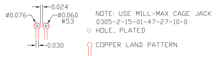
Less conservative, but more convenient in many applications, is the use of cage jacks that provide the same function as a socket. The amplifier may be removed easily from the mother board but the pin to pin spacing is reduced owing to the diameter of the cage jack. The Mill-Max cage jacks provided in Power Amp Design’s evaluation kits is assumed for Figure 2. The PCB top side pad is the same diameter as the cage jack. This provides no annular ring around the cage jack head but the cage jack is to be used with plated-through holes and the cage jack is soldered from the opposite side of the PCB where sufficient annular ring is provided. Solder mask may be added in addition.
Either of the approaches as illustrated in Figures 1 and 2 have been shown to work well in field applications as outlined above. It should be noted, in addition, that PCB traces elsewhere on the mother board need to be analyzed as well. Outside and inside corners in the mother board traces should have a radius of 0.005” or more. Following these guide lines will provide a reliable application circuit.